SLVS817G May 2008 – June 2015 TPD4S009 , TPD4S010
PRODUCTION DATA.
- 1 Features
- 2 Applications
- 3 Description
- 4 Revision History
- 5 Pin Configuration and Functions
- 6 Specifications
-
7 Detailed Description
- 7.1 Overview
- 7.2 Functional Block Diagram
- 7.3
Feature Description
- 7.3.1 ±8-kV IEC61000-4-2 Level 4 Contact ESD Protection
- 7.3.2 IEC61000-4-5 Surge Protection
- 7.3.3 I/O Capacitance
- 7.3.4 Low Leakage Current
- 7.3.5 Supports High-Speed Differential Data Rates
- 7.3.6 Ultra-low Matching Capacitance Between Differential Signal Pairs
- 7.3.7 Ioff Feature for the TPD4S009
- 7.3.8 Industrial Temperature Range
- 7.3.9 Easy Flow-Through Routing
- 7.4 Device Functional Modes
- 8 Application and Implementation
- 9 Power Supply Recommendations
- 10Layout
- 11Device and Documentation Support
- 12Mechanical, Packaging, and Orderable Information
パッケージ・オプション
メカニカル・データ(パッケージ|ピン)
サーマルパッド・メカニカル・データ
- DRY|6
発注情報
8 Application and Implementation
NOTE
Information in the following applications sections is not part of the TI component specification, and TI does not warrant its accuracy or completeness. TI’s customers are responsible for determining suitability of components for their purposes. Customers should validate and test their design implementation to confirm system functionality.
8.1 Application Information
TPD4S009 and TPD4S010 are four-channel TVS diode arrays which are used to provide IEC 61000-4-2 system level ESD protection for a human interface connector. TPD4S009 and TPD4S010 provide a path to ground for dissipating ESD events on hi-speed signal lines between the human interface connector and the system. As the current from ESD passes through the TVS, only a small voltage drop is present across the diode. This is the voltage presented to the protected IC. The low RDYN of the triggered TVS holds this voltage, VCLAMP, to a safe level for the protected IC.
8.2 Typical Application
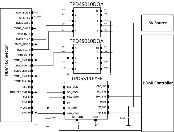
 Figure 8. Typical Application Schematic
8.2.1 Design Requirements
For this design example, two TPD4S010 devices, and one TPD5S116 are being used in an HDMI 1.4 application. This will provide a complete port protection scheme.
Given the HDMI 1.4 application, the following parameters are known.
| DESIGN PARAMETER | VALUE |
|---|---|
| Signal range on Pins 1, 2, 4, or 5 | 0 V to 3.6 V |
| Operating Frequency | 1.7 GHz |
8.2.2 Detailed Design Procedure
To begin the design process, some parameters must be decided upon; the designer needs to know the following:
- Signal range on all the protected lines
- Operating frequency
8.2.2.1 Signal Range on Pin 1, 2, 4, or 5
TPD4S010 has 4 identical protection channels for signal lines. The symmetry of the device provides flexibility when selecting which of the 4 I/O channels will protect which signal lines. Any I/O will support a signal range of 0 to 5.5 V. Therefore, this device will support the HDMI 1.4 signal swing.
8.2.2.2 Bandwidth on Pin 1, 2, 4, or 5
Each pin of the TPD4S010 has a typical –3 dB bandwidth of 4GHz. Therefore, this device can handle HDMI 1.4 data rate of 3.4 Gbps with operating frequency of 1.7 GHz.

