SLVSBP3C December 2012 – May 2015 TPD5S116
PRODUCTION DATA.
- 1 Features
- 2 Applications
- 3 Description
- 4 Simplified Schematic
- 5 Revision History
- 6 Pin Configuration and Functions
-
7 Specifications
- 7.1 Absolute Maximum Ratings
- 7.2 ESD Ratings
- 7.3 Recommended Operating Conditions
- 7.4 Thermal Information
- 7.5 Electrical Characteristics
- 7.6 Voltage Level Shifter, SCL, SDA Lines
- 7.7 Voltage Level Shifter, CEC Line
- 7.8 Voltage Level Shifter, HPD Line
- 7.9 EN
- 7.10 Utility Pin
- 7.11 I/O Capacitances
- 7.12 Dynamic Load Characteristics
- 7.13 SCL, SDA Lines, VCCA = 1.2 V
- 7.14 CEC Line, VCCA = 1.2 V
- 7.15 HPD Line, VCCA = 1.2 V
- 7.16 SCL, SDA Lines, VCCA = 1.5 V
- 7.17 CEC Line, VCCA = 1.5 V
- 7.18 HPD Line, VCCA = 1.5 V
- 7.19 SCL, SDA Lines, VCCA = 1.8 V
- 7.20 CEC Line, VCCA = 1.8 V
- 7.21 HPD Line, VCCA = 1.8 V
- 7.22 SCL, SDA Lines, VCCA = 2.5 V
- 7.23 CEC Line, VCCA = 2.5 V
- 7.24 HPD Line, VCCA = 2.5 V
- 7.25 SCL, SDA Lines, VCCA = 3.3 V
- 7.26 CEC Line, VCCA = 3.3 V
- 7.27 HPD Line, VCCA = 3.3 V
- 7.28 SCL, SDA Lines, VCCA = 5 V
- 7.29 CEC Line, VCCA = 5 V
- 7.30 HPD Line, VCCA = 5 V
- 7.31 Typical Characteristics
-
8 Detailed Description
- 8.1 Overview
- 8.2 Functional Block Diagram
- 8.3
Feature Description
- 8.3.1 IEC 61000-4-2 Level 4 ESD Protection
- 8.3.2 Conforms to HDMI Control and 5VOUT Compliance Tests Without External Components
- 8.3.3 Auto-direction Sensing I2C Level Shifter with One-Shot Circuit to Drive Long HDMI Cable (750-pF Load)
- 8.3.4 Back Drive Protection
- 8.3.5 55-mA Load Switch with Short Circuit Protection
- 8.3.6 Hot Plug Detect Module with Pull Down Resistor
- 8.3.7 Integrated Pull-up and Pull-down Resistors per HDMI Specification
- 8.3.8 Utility Pin ESD Protection for Ethernet and Audio Return
- 8.3.9 DDC/CEC LEVEL SHIFT Circuit Operation
- 8.3.10 DDC/CEC Level Shifter Operational Notes For VCCA = 1.8V
- 8.3.11 Rise-Time Accelerators
- 8.3.12 Noise Considerations
- 8.3.13 HDMI Compliance
- 8.4 Device Functional Modes
- 9 Applications and Implementations
- 10Power Supply Requirements
- 11Layout
- 12Device and Documentation Support
- 13Mechanical, Packaging, and Orderable Information
11 Layout
11.1 Layout Guidelines
- The optimum placement is as close to the connector as possible.
- EMI during an ESD event can couple from the trace being struck to other nearby unprotected traces, resulting in early system failures. Therefore, the PCB designer needs to minimize the possibility of EMI coupling by keeping any unprotected traces away from the protected traces which are between the TVS and the connector.
- Route the protected traces as straight as possible.
- Avoid using VIAs between the connecter and an I/O protection pin on TPD5S116.
- Avoid 90º turns in traces.
- Electric fields tend to build up on corners, increasing EMI coupling.
- Minimize impedance on the path to GND for maximum ESD dissipation.
- The capacitors on 5V_CON and 5V_SYS should be placed close to their respective pins on TPD5S116.
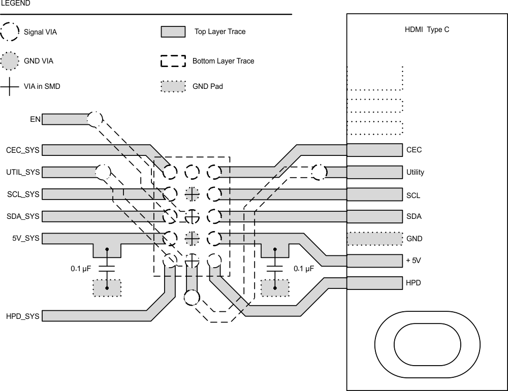
11.2 Layout Example
 Figure 22. TPD5S116 HDMI Layout Example