SNAS628B JULY 2013 – December 2014 TPL5000
PRODUCTION DATA.
- 1 Features
- 2 Applications
- 3 Description
- 4 Simplified Application Schematic
- 5 Revision History
- 6 Pin Configuration and Functions
- 7 Specifications
- 8 Detailed Description
- 9 Application and Implementation
- 10Power Supply Recommendations
- 11Layout
- 12Device and Documentation Support
- 13Mechanical, Packaging, and Orderable Information
7 Specifications
7.1 Absolute Maximum Ratings
over operating free-air temperature (unless otherwise noted) (1)| MIN | MAX | UNIT | ||
|---|---|---|---|---|
| Supply Voltage | –0.3 | 6.0 | V | |
| Input Voltage(2) | –0.3 | VDD + 0.3 | V | |
| Voltage between any two pins | VDD + 0.3 | V | ||
| Input Current on any pin | –5 | 5 | mA | |
| Operating Temperature, TA | –40 | 105 | ||
| Junction Temperature, TJ(3) | 150 | °C | ||
| Storage Temperature, Tstg | –65 | 150 | °C | |
(1) Stresses beyond those listed under Absolute Maximum Ratings may cause permanent damage to the device. These are stress ratings only, which do not imply functional operation of the device at these or any other conditions beyond those indicated under Recommended Operating Conditions. Exposure to absolute-maximum-rated conditions for extended periods may affect device reliability.
(2) When the input voltage (VIN) at any pin exceeds the power supply (VDD), the current on that pin must not exceed 5 mA and must not exceed 6.0 V.
(3) The maximum power dissipation is a function of TJ(MAX), RθJA, and the ambient temperature, TA. The maximum allowable power dissipation at any ambient temperature is PDMAX = (TJ(MAX) - TA)/ θJA. All numbers apply for packages soldered directly onto a PCB.
7.2 ESD Ratings
| VALUE | UNIT | |||
|---|---|---|---|---|
| V(ESD) | Electrostatic discharge | Human-body model (HBM), per ANSI/ESDA/JEDEC JS-001(1) | ±2000 | V |
| Charged-device model (CDM), per JEDEC specification JESD22-C101(2) | ±500 | |||
(1) JEDEC document JEP155 states that 500-V HBM allows safe manufacturing with a standard ESD control process.
(2) JEDEC document JEP157 states that 250-V CDM allows safe manufacturing with a standard ESD control process.
7.3 Recommended Operating Ratings
| MIN | MAX | UNIT | ||||
|---|---|---|---|---|---|---|
| Supply Voltage (VDD-GND) | 1.8 | 5.0 | V | |||
| Temperature Range | -40 | 105 | °C | |||
7.4 Thermal Information
| THERMAL METRIC(1) | TPL5000 | UNIT | |
|---|---|---|---|
| VSSOP | |||
| 10 PINS | |||
| RθJA | Junction-to-ambient thermal resistance | 196.8 | °C/W |
(1) For more information about traditional and new thermal metrics, see the IC Package Thermal Metrics application report, SPRA953.
7.5 Electrical Characteristics(1)
Specifications are for TA =TJ = 25°C, VDD-GND=2.5 V, unless otherwise stated.| PARAMETER | TEST CONDITIONS | MIN(2) | TYP(3) | MAX(2) | UNIT | |
|---|---|---|---|---|---|---|
| POWER SUPPLY | ||||||
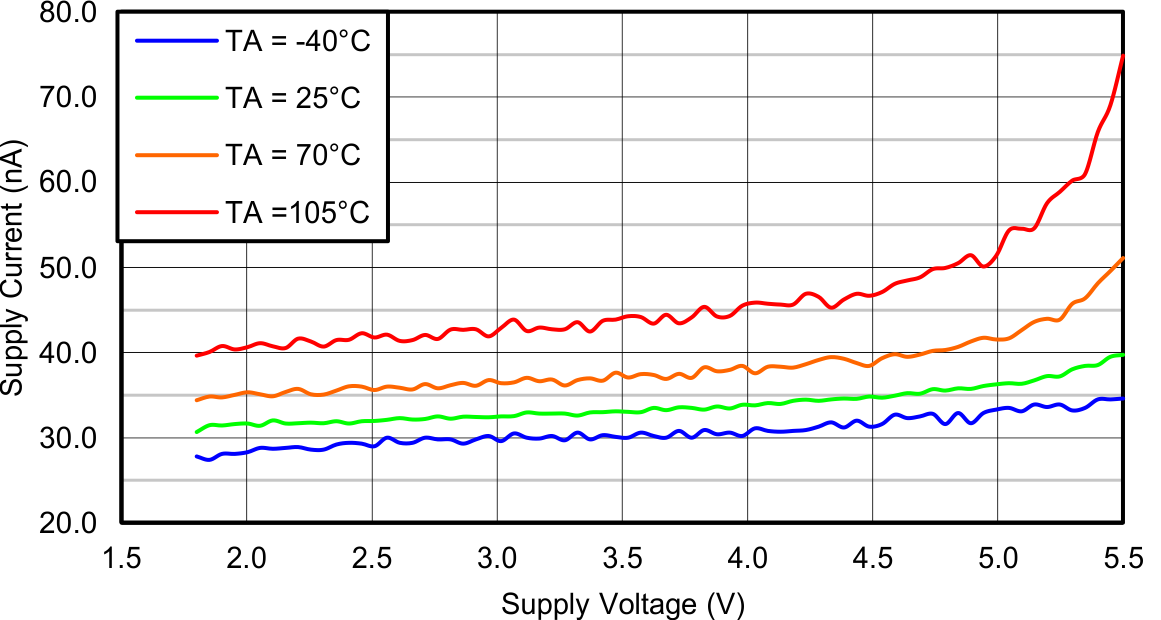
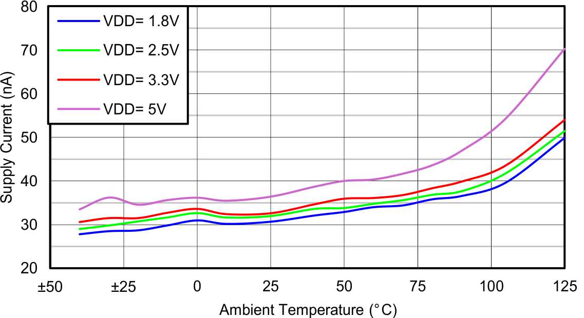
| IVDD | Supply current(4) | PGOOD = VDD | 30 | 50 | nA | |
| PGOOD = GND | 12 | nA | ||||
| TIMER | ||||||
| tDP | Timer Delay Period | 1, 2, 4, 8, 10, 16, 32, 64 | s | |||
| Timer Delay drift over life time(6) | 0.06% | |||||
| Timer Delay drift over temperature | 400 | ppm/°C | ||||
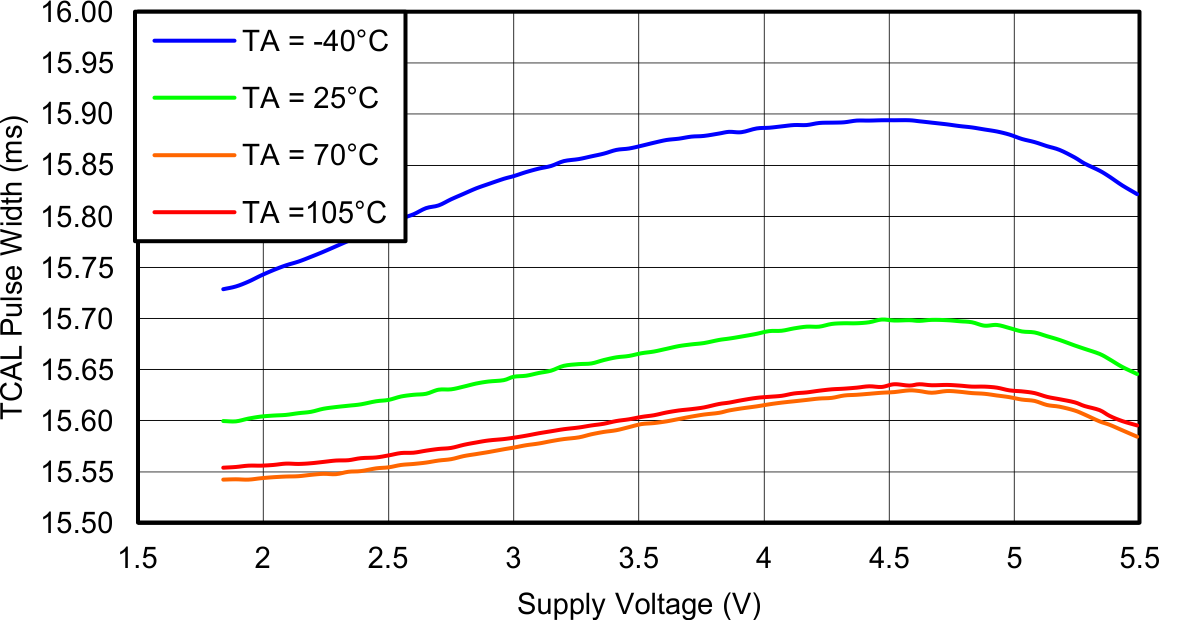
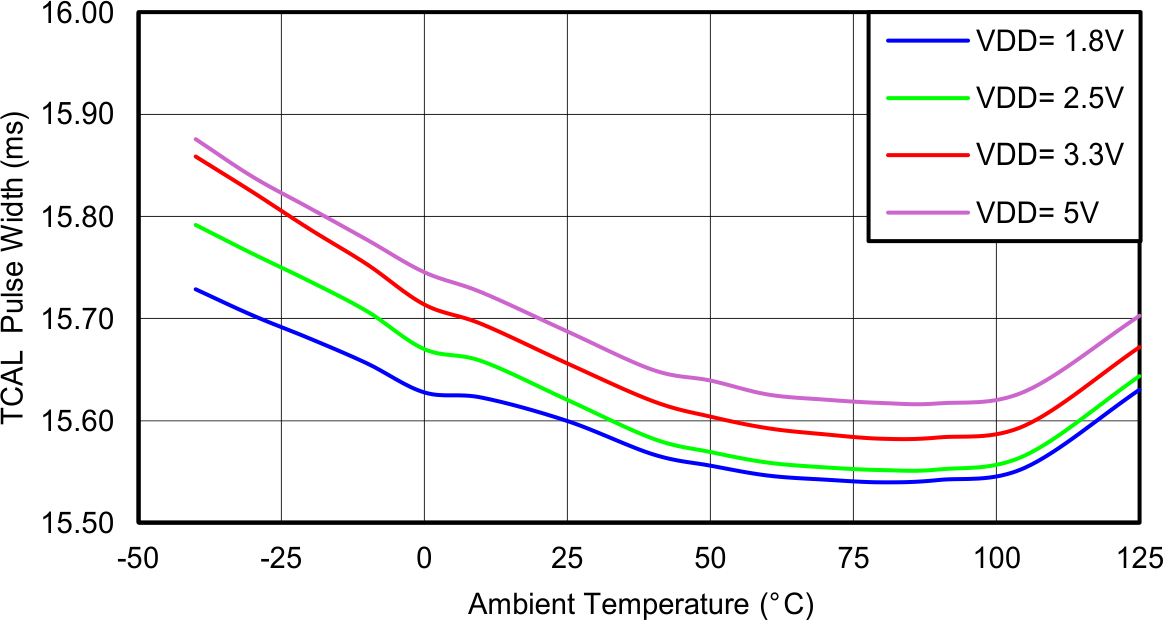
| tCAL | Calibration pulse width | 14.063 | 15.625 | 17.188 | ms | |
| tDP to tCAL matching error(5) | VDD ≤ 3.0 V | 0.1 | ||||
| tDONE | DONE Pulse width (5) | 100 | ns | |||
| tRSTn | RSTn Pulse width | 15.625 | ms | |||
| tWAKE | WAKE Pulse width | 31.25 | ms | |||
| DIGITAL LOGIC LEVELS | ||||||
| VIH | Logic High Threshold | PGOOD, DONE | 0.7xVDD | V | ||
| VIL | Logic Low Threshold | PGOOD, DONE | 0.3xVDD | V | ||
| VOH | Logic output High Level | WAKE, TCAL Iout = 100 uA |
VDD-0.3 | V | ||
| WAKE, TCAL Iout = 1 mA |
VDD-0.7 | V | ||||
| VOL | Logic output Low Level | WAKE, TCAL Iout = -100 uA |
0.3 | V | ||
| WAKE, TCAL Iout = -1 mA |
0.7 | V | ||||
| VOLRSTn | RSTn Logic output Low Level | IOL= -1 mA | 0.3 | V | ||
| IOHRSTn | RSTn High Level output current | VOHRSTn=VDD | 1 | nA | ||
(1) Electrical Characteristics Table values apply only for factory testing conditions at the temperature indicated. Factory testing conditions result in very limited self-heating of the device such that TJ = TA.
(2) Limits are specified by testing, design, or statistical analysis at 25°C. Limits over the operating temperature range are specified through correlations using statistical quality control (SQC) method.
(3) Typical values represent the most likely parametric norm as determined at the time of characterization. Actual typical values may vary over time and will also depend on the application and configuration. The typical values are not tested and are not specified on shipped production material.
(4) The supply current does not take in account load and pull-up resistor current. Input pins are at GND or VDD.
(5) Ensured by design.
(6) Operational life time test procedure equivalent to10 years.
7.6 Timing Requirements
| MIN | TYP | MAX | UNIT | ||||
|---|---|---|---|---|---|---|---|
| trTCAL | Rise Time TCAL | Capacitive load 15 pF | 50 | ns | |||
| tfTCAL, | Fall Time TCAL | Capacitive load 15 pF | 50 | ns | |||
| trRSTn, | Rise Time RSTn | Capacitive load 15 pF, Rpull-up 100Kohm | 4 | ns | |||
| tfRSTn, | Fall Time RSTn | Capacitive load 15 pF, Rpull-up 100Kohm | 50 | ns | |||
| trWAKE | Rise Time WAKE | Capacitive load 15 pF | 50 | ns | |||
| tfWAKE | Fall Time WAKE | Capacitive load 15 pF | 50 | ns | |||
| tDDONE | DONE to RSTn or WAKE delay | Min delay | 100 | ns | |||
| Max delay | tDP-5*tCAL | ms | |||||
| tDTCAL | TCAL to RSTn or WAKE delay | tCAL/2 | ms | ||||
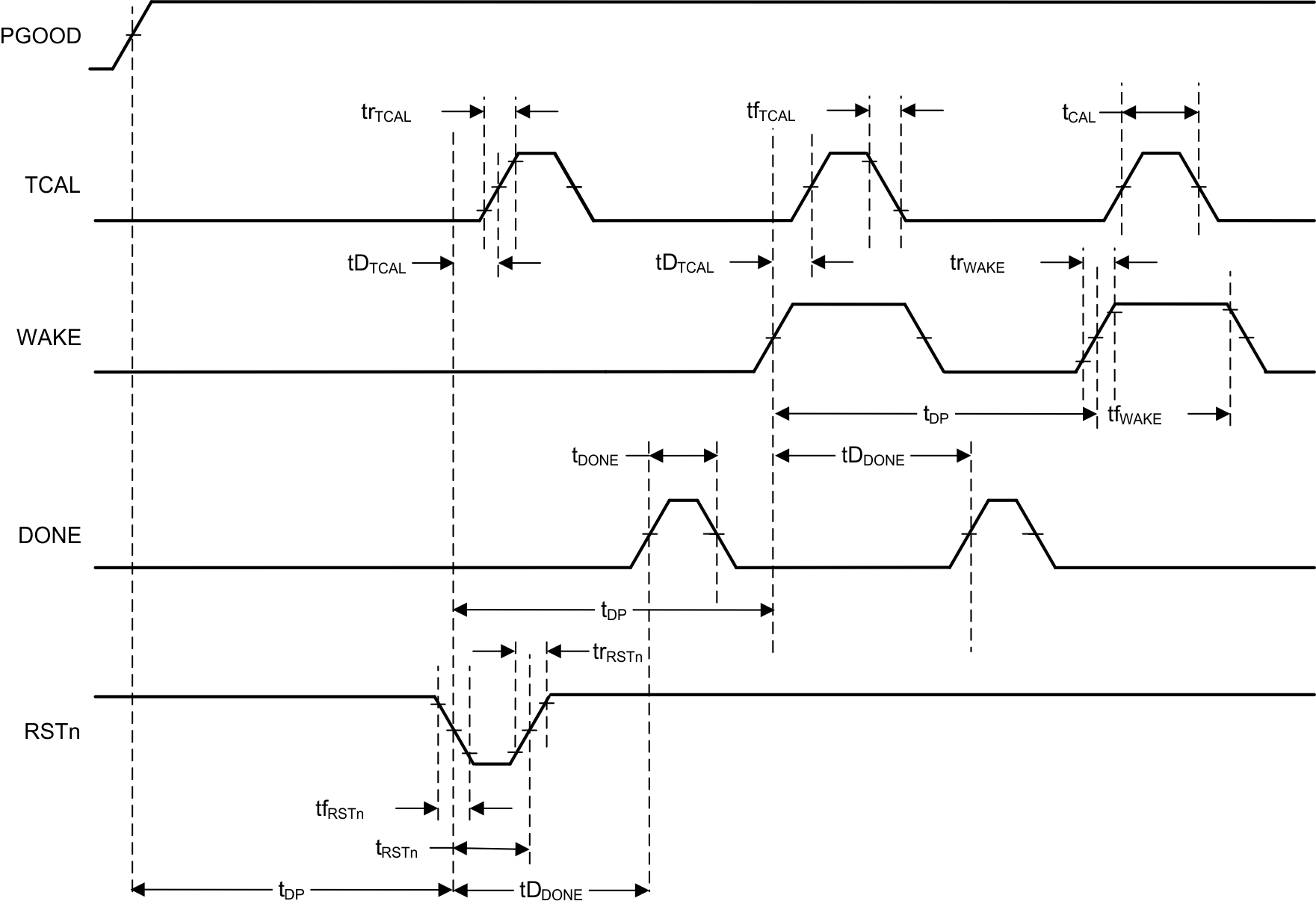 Figure 1. Timing Diagram
7.7 Typical Characteristics