JAJSER0D February   2018  – September 2021 TPS1H200A-Q1

PRODUCTION DATA  

  1. 特長
  2. アプリケーション
  3. 概要
  4. Revision History
  5. Pin Configuration and Functions
  6. Specifications
    1. 6.1 Absolute Maximum Ratings
    2. 6.2 ESD Ratings
    3. 6.3 Recommended Operating Conditions
    4. 6.4 Thermal Information
    5. 6.5 Electrical Characteristics
    6. 6.6 Switching Characteristics
    7. 6.7 Typical Characteristics
  7. Detailed Description
    1. 7.1 Overview
    2. 7.2 Functional Block Diagram
    3. 7.3 Feature Description
      1. 7.3.1 Current limit
      2. 7.3.2 DELAY Pin Configuration
        1. 7.3.2.1 Holding Mode
        2. 7.3.2.2 Latch-Off Mode
        3. 7.3.2.3 Auto-Retry Mode
      3. 7.3.3 Stand-alone Operation
      4. 7.3.4 Fault Truth Table
      5. 7.3.5 Full Diagnostics
        1. 7.3.5.1 Short-to-GND and Overload Detection
        2. 7.3.5.2 Open-Load Detection
          1. 7.3.5.2.1 Output On
          2. 7.3.5.2.2 Output Off
        3. 7.3.5.3 Short-to-Battery Detection
        4. 7.3.5.4 Thermal Fault Detection
          1. 7.3.5.4.1 Thermal Shutdown
          2. 7.3.5.4.2 Thermal Swing
          3. 7.3.5.4.3 Fault Report Holding
      6. 7.3.6 Full Protections
        1. 7.3.6.1 UVLO Protection
        2. 7.3.6.2 Inductive Load Switching Off Clamp
        3. 7.3.6.3 Loss-of-GND Protection
        4. 7.3.6.4 Loss-of-Power-Supply Protection
        5. 7.3.6.5 Reverse-Current Protection
        6. 7.3.6.6 MCU I/O Protection
    4. 7.4 Device Functional Modes
      1. 7.4.1 Working Modes
        1. 7.4.1.1 Normal Mode
        2. 7.4.1.2 Standby Mode
        3. 7.4.1.3 Standby Mode With Diagnostics
  8. Application and Implementation
    1. 8.1 Application Information
    2. 8.2 Typical Application
      1. 8.2.1 Design Requirements
      2. 8.2.2 Detailed Design Procedure
      3. 8.2.3 Application Curves
  9. Power Supply Recommendations
  10. 10Layout
    1. 10.1 Layout Guidelines
    2. 10.2 Layout Example
  11. 11Device and Documentation Support
    1. 11.1 Documentation Support
      1. 11.1.1 Related Documentation
    2. 11.2 Receiving Notification of Documentation Updates
    3. 11.3 サポート・リソース
    4. 11.4 Trademarks
    5. 11.5 Electrostatic Discharge Caution
    6. 11.6 Glossary
  12. 12Mechanical, Packaging, and Orderable Information

パッケージ・オプション

メカニカル・データ(パッケージ|ピン)
サーマルパッド・メカニカル・データ
発注情報

Reverse-Current Protection

Reverse current occurs in two conditions: short to supply and reverse polarity.

  • When a short to the supply occurs, there is only reverse current through the body diode. IR(1) specifies the limit of the reverse current.
  • In a reverse-polarity condition, there are reverse currents through the body diode and the device GND pin. IR(2) specifies the limit of the reverse current.

To protect the device, TI recommends using two types of external circuitry.

  • Adding a blocking diode (method 1). The device and load are protected when in reverse polarity.
  • Adding a GND network (method 2). The reverse current through the device GND is blocked. The reverse current through the FET is limited by the load itself. TI recommends a resistor in parallel with the diode as a GND network. The recommended configuration is a 1-kΩ resistor in parallel with a diode that is less than 100 mA.
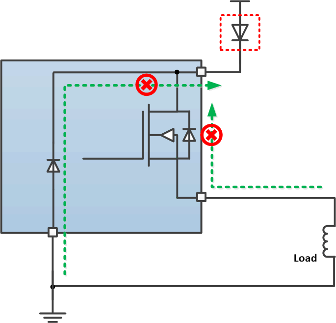
GUID-8DF0C0B4-8BAD-45C2-8779-B4ECC733B12C-low.gifFigure 7-17 Reverse-Current External Protection Method 1
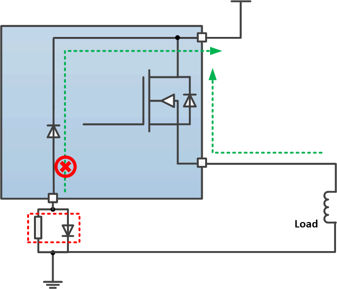
GUID-0E595DCE-8334-44FE-843B-99F8FEB2684E-low.gifFigure 7-18 Reverse-Current External Protection Method 2