JAJSG28F august 2018 – august 2020 TPS2120 , TPS2121
PRODUCTION DATA
- 1
- 1 特長
- 2 アプリケーション
- 3 概要
- 4 Revision History
- 5 Device Comparison Table
- 6 Pin Configuration and Functions
- 7 Specifications
- 8 Parameter Measurement Information
-
9 Detailed Description
- 9.1 Overview
- 9.2 Functional Block Diagram
- 9.3
Feature Description
- 9.3.1 Input Settling Time and Output Soft Start Control (SS)
- 9.3.2 Active Current Limiting (ILM)
- 9.3.3 Short-Circuit Protection
- 9.3.4 Thermal Protection (TSD)
- 9.3.5 Overvoltage Protection (OVx)
- 9.3.6 Fast Reverse Current Blocking (RCB)
- 9.3.7 Output Voltage Dip and Fast Switchover Control (TPS2121 only)
- 9.3.8 Input Voltage Comparator (VCOMP)
- 9.4 TPS2120 Device Functional Modes
- 9.5 TPS2121 Device Functional Modes
- 10Application and Implementation
- 11Power Supply Recommendations
- 12Layout
- 13Device and Documentation Support
- 14Mechanical, Packaging, and Orderable Information
パッケージ・オプション
デバイスごとのパッケージ図は、PDF版データシートをご参照ください。
メカニカル・データ(パッケージ|ピン)
- RUX|12
サーマルパッド・メカニカル・データ
発注情報
10.6 Reverse Polarity Protection with TPS212x
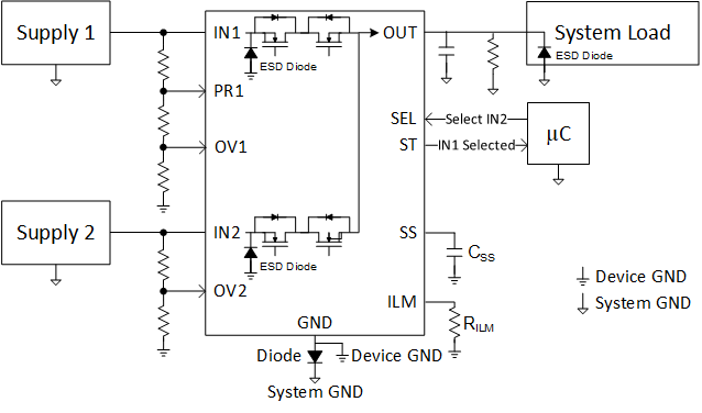
For applications that require reverse polarity protection, the TPS212x can be configured to protect against mis-wiring input power supplies and block reverse current that could potentially damage the system. By connecting a diode on the GND pin of the TPS212x, this prevents reverse current from flowing back into the device when VIN is below system ground.
Since the TPS212x has an absolute maximum rating of 24 V when referenced to device ground, the GND diode should be rated to standoff voltages up to the maximum reverse voltage. Furthermore, since the control pin voltages (PR1, OV1, OV2, etc.) are in reference to system GND, the voltage thresholds will need to be recalculated based on the voltage drop across the diode. To reduce the voltage drop, a resistor in parallel with the diode can also be used.
 Figure 10-19 TPS212x Reverse Polarity Configuration