SLVSAY8D June 2011 – January 2016 TPS22920
PRODUCTION DATA.
- 1 Features
- 2 Applications
- 3 Description
- 4 Revision History
- 5 Device Comparison Table
- 6 Pin Configuration and Functions
-
7 Specifications
- 7.1 Absolute Maximum Ratings
- 7.2 ESD Ratings
- 7.3 Recommended Operating Conditions
- 7.4 Thermal Information
- 7.5 Electrical Characteristics
- 7.6 Switching Characteristics: VIN = 3.6 V
- 7.7 Switching Characteristics: VIN = 0.9 V
- 7.8 Typical DC Characteristics
- 7.9 TPS22920 Typical AC Characteristics
- 7.10 TPS22920L Typical AC Characteristics
- 8 Parametric Measurement Information
- 9 Detailed Description
- 10Application and Implementation
- 11Power Supply Recommendations
- 12Layout
- 13Device and Documentation Support
- 14Mechanical, Packaging, and Orderable Information
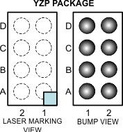
6 Pin Configuration and Functions
8-PIN

Pin Functions
| PIN | I/O | DESCRIPTION | |
|---|---|---|---|
| NAME | NO. | ||
| GND | D1 | - | Ground |
| ON | D2 | I | Switch control input. Do not leave floating |
| VOUT | A1, B1, C1 | O | Switch output |
| VIN | A2, B2, C2 | I | Switch input, bypass this input with a ceramic capacitor to ground |
Table 1. Bump Assignments (YZP Package)
| D | GND | ON |
| C | VOUT | VIN |
| B | VOUT | VIN |
| A | VOUT | VIN |
| 1 | 2 |