SLVS788D February 2009 – November 2016 TPS22951
PRODUCTION DATA.
- 1 Features
- 2 Applications
- 3 Description
- 4 Revision History
- 5 Pin Configurations and Functions
- 6 Specifications
- 7 Parameter Measurement Information
- 8 Detailed Description
- 9 Application and Implementation
- 10Power Supply Recommendations
- 11Layout
- 12Device and Documentation Support
- 13Mechanical, Packaging, and Orderable Information
11 Layout
11.1 Layout Guidelines
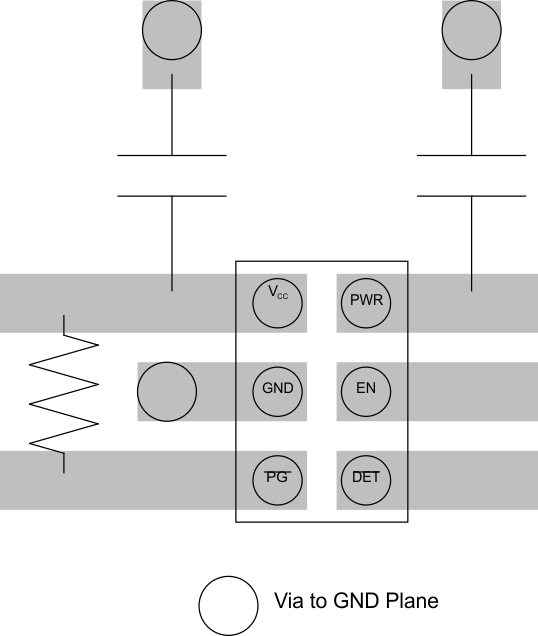
- The VCC and PWR traces must be wide enough to carry the necessary load current (up to 600 mA).
- To handle transient load currents, a capacitor may be placed close to the VCC pin.
- To make use of the PG signal, it must be connected to a pullup resistor. The pullup source may be the VCC node. It is also possible to use a different source for the pullup resistor.
11.2 Layout Example
 Figure 14. Layout Example
11.3 Thermal Considerations
The maximum IC junction temperature must be restricted to 85°C under normal operating conditions. To calculate the maximum allowable dissipation, PD(max) for a given ambient temperature, use Equation 2 and Equation 3.
Equation 2. 

where
- PD(max) = maximum allowable power dissipation
- TJ(max) = maximum allowable junction temperature (85°C for the TPS22951)
- TA = ambient temperature of the device
- RθJA = junction to air thermal impedance. See thermal metrics table. This parameter is highly dependent upon board layout.
Equation 3. PD = I2 × R