SLVSCI4B February 2014 – September 2014 TPS22961
PRODUCTION DATA.
- 1 Features
- 2 Applications
- 3 Description
- 4 Simplified Schematic
- 5 Revision History
- 6 Terminal Configuration and Functions
- 7 Specifications
- 8 Detailed Description
- 9 Applications and Implementation
- 10Power Supply Recommendations
- 11Layout
- 12Device and Documentation Support
- 13Mechanical, Packaging, and Orderable Information
パッケージ・オプション
デバイスごとのパッケージ図は、PDF版データシートをご参照ください。
メカニカル・データ(パッケージ|ピン)
- DNY|8
サーマルパッド・メカニカル・データ
発注情報
9 Applications and Implementation
NOTE
Information in the following applications sections is not part of the TI component specification, and TI does not warrant its accuracy or completeness. TI’s customers are responsible for determining suitability of components for their purposes. Customers should validate and test their design implementation to confirm system functionality.
9.1 Application Information
This section will highlight some of the design considerations when implementing this device in various applications. A PSPICE model for this device is also available in the product page of this device on www.ti.com for further aid.
9.2 Typical Application
9.2.1 Typical Application Powering a Downstream Module
This application demonstrates how the TPS22961 can be used to power downstream modules.
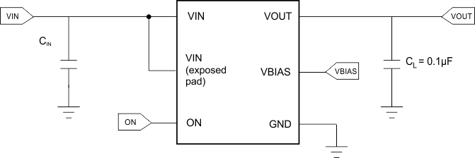 Figure 26. Typical Application Schematic for Powering a Downstream Module
9.2.1.1 Design Requirements
For this design example, use the following as the input parameters.
Table 1. Design Parameters
| DESIGN PARAMETER | EXAMPLE VALUE |
|---|---|
| VIN | 1.05 V |
| VBIAS | 5.0 V |
| Load current | 6 A |
9.2.1.2 Detailed Design Procedure
To begin the design process, the designer needs to know the following:
- VIN voltage
- VBIAS voltage
- Load current
9.2.1.2.1 VIN to VOUT Voltage Drop
The VIN to VOUT voltage drop in the device is determined by the RON of the device and the load current. The RON of the device depends upon the VIN and VBIAS conditions of the device. Refer to the RON specification of the device in the Electrical Characteristics table of this datasheet. Once the RON of the device is determined based upon the VIN and VBIAS conditions, use Equation 1 to calculate the VIN to VOUT voltage drop:
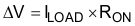
where
- ΔV = voltage drop from VIN to VOUT
- ILOAD = load current
- RON = On-resistance of the device for a specific VIN and VBIAS combination
An appropriate ILOAD must be chosen such that the IMAX specification of the device is not violated.
9.2.1.2.2 Inrush Current
To determine how much inrush current will be caused by the CL capacitor, use Equation 2:
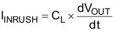
where
- IINRUSH = amount of inrush caused by CL
- CL = capacitance on VOUT
- dt = time it takes for change in VOUT during the ramp up of VOUT when the device is enabled
- dVOUT = change in VOUT during the ramp up of VOUT when the device is enabled
An appropriate CL value should be placed on VOUT such that the IMAX and IPLS specficiations of the device are not violated.
9.2.1.2.3 Thermal Considerations
The maximum IC junction temperature should be restricted to 125°C under normal operating conditions. To calculate the maximum allowable dissipation, PD(max) for a given output current and ambient temperature, use Equation 3.
where
- PD(max) = maximum allowable power dissipation
- TJ(max) = maximum allowable junction temperature (125°C for the TPS22961)
- TA = ambient temperature of the device
- ΘJA = junction to air thermal impedance. See Thermal Information section. This parameter is highly dependent upon board layout.
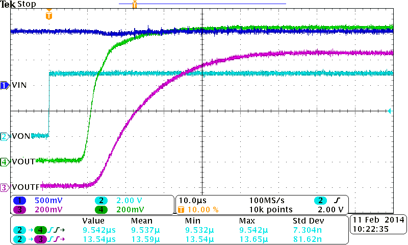
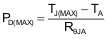
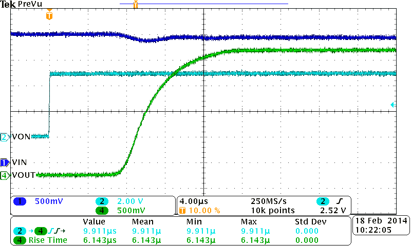
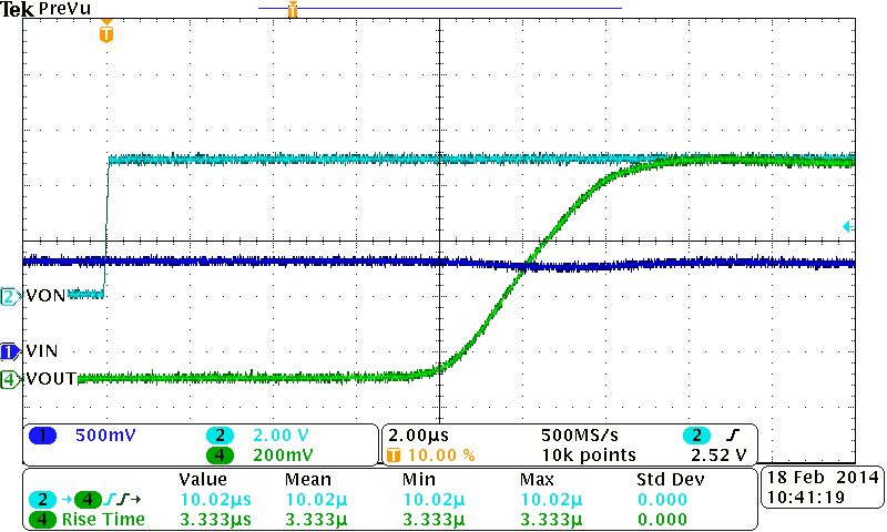
9.2.1.3 Application Curves
| VBIAS = 5 V | VIN = 2.5 V | CIN = 1 µF |
| CL = 0.1 µF |
| VBIAS = 5 V | VIN = 1.05 V | CIN = 1 µF |
| CL = 0.1 µF |
| VBIAS = 5 V | VIN = 0.8 V | CIN = 1 µF |
| CL = 0.1 µF |
| VBIAS = 5 V | VIN = 0.8 V | CIN = 1 µF |
| CL = 0.1 µF |
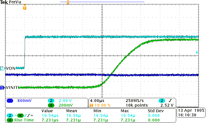
9.2.2 Typical Application Powering Rails Sensitive to Ringing and Overvoltage due to Fast Rise Time
This application demonstrates how the TPS22961 can be used to power rails senstive to ringing and overvoltage that can often happen due to fast rise times.
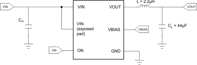 Figure 31. Typical Application Schematic for Powering Rails Sensitive to Ringing
9.2.2.1 Design Requirements
For this design example, use the following as the input parameters.
Table 2. Design Parameters
| DESIGN PARAMETER | EXAMPLE VALUE |
|---|---|
| VIN | 1.05 V |
| VBIAS | 5.0 V |
| Acceptable percent overshoot (ρ) | 3.2% |
| Maximum settling time (tSETTLE) | 40 µs |
9.2.2.2 Detailed Design Procedure
To begin the design process, the designer needs to know the following:
- VIN voltage
- VBIAS voltage
- Acceptable percent overshoot
- Maximum allowed settling time for the power rail
9.2.2.2.1 Picking Proper Inductor and Capacitor to Meet Voltage Overshoot Requirements
To determine the value of L and CL in the circuit, the damping factor associated with the acceptable percent overshoot must be calculated. To calculate the damping factor (ε), use Equation 4.
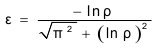
where
- ε = damping factor of the LC filter
- ρ = allowable percent overshoot for the power rail
Use the damping factor calculated in Equation 4 to determine the inductance (L), the DCR of the inductor (RDCR), and capacitance (CL) to achieve the percent overshoot. This will be an iterative process to determine the optimal combination of L and CL with standard value components available. Use Equation 5 to determine the combination of L, RDCR, and CL that is needed to satisfy damping factor calculated from Equation 4.

where
- ε = damping factor of the LC filter
- RDCR = DCR of the inductor
- CL = the capacitance of the filter
- L = the inductor of the filter
To determine the setting time (within 5% of steady state value) of the filter, use Equation 6.
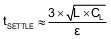
where
- tSETTLE = settling time of filter to within 5% of steady state value
- ε = damping factor of the LC filter
- CL = the capacitance of the filter
- L = the inductor of the filter
The combination of damping factor (ε) and filter settling time (tSETTLE) will bound the values for L, RDCR, and CL that can be used to meet the design constraints in Table 2.