JAJSIO1B December 2013 – March 2020 TPS22966-Q1
PRODUCTION DATA.
- 1 特長
- 2 アプリケーション
- 3 概要
- 4 改訂履歴
- 5 Pin Configuration and Functions
- 6 Specifications
- 7 Parameter Measurement Information
- 8 Detailed Description
- 9 Application and Implementation
- 10Power Supply Recommendations
- 11Layout
- 12デバイスおよびドキュメントのサポート
- 13メカニカル、パッケージ、および注文情報
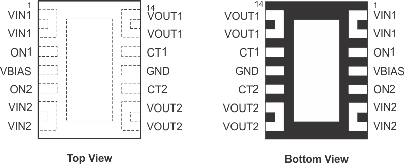
5 Pin Configuration and Functions
DPU Package
14-Pin WSON

Pin Functions
| PIN | I/O | DESCRIPTION | |
|---|---|---|---|
| NO. | NAME | ||
| 1 | VIN1 | I | Switch 1 input. Place an optional decoupling capacitor between this pin and GND for reduce VIN dip during turnon of the channel. See Application Information section for more information. |
| 2 | VIN1 | I | Switch 1 input. Place an optional decoupling capacitor between this pin and GND for reduce VIN dip during turnon of the channel. See Application Informationfor more information. |
| 3 | ON1 | I | Active high switch 1 control input. Do not leave floating. |
| 4 | VBIAS | I | Bias voltage. Power supply to the device. See Application Information for more information. |
| 5 | ON2 | I | Active high switch 2 control input. Do not leave floating. |
| 6 | VIN2 | I | Switch 2 input. Place an optional decoupling capacitor between this pin and GND for reduce VIN dip during turnon of the channel. See Application Information for more information. |
| 7 | VIN2 | I | Switch 2 input. Place an optional decoupling capacitor between this pin and GND for reduce VIN dip during turnon of the channel. See Application Information for more information. |
| 8 | VOUT2 | O | Switch 2 output. |
| 9 | VOUT2 | O | Switch 2 output. |
| 10 | CT2 | O | Switch 2 slew rate control. Can be left floating. Capacitor used on this pin should be rated for a minimum of 25 V for desired rise time performance. |
| 11 | GND | – | Ground |
| 12 | CT1 | O | Switch 1 slew rate control. Can be left floating. Capacitor used on this pin should be rated for a minimum of 25 V for desired rise time performance. |
| 13 | VOUT1 | O | Switch 1 output. |
| 14 | VOUT1 | O | Switch 1 output. |
| 15 | Thermal Pad | O | Thermal pad (exposed center pad) to alleviate thermal stress. Tie to GND. See Layout Guidelines for layout guidelines. |