SLVSBM6B December 2012 – November 2015 TPS22981
PRODUCTION DATA.
- 1 Features
- 2 Applications
- 3 Description
- 4 Revision History
- 5 Pin Configuration and Functions
- 6 Specifications
- 7 Detailed Description
- 8 Application and Implementation
- 9 Power Supply Recommendations
- 10Layout
- 11Device and Documentation Support
- 12Mechanical, Packaging, and Orderable Information
パッケージ・オプション
メカニカル・データ(パッケージ|ピン)
- RGP|20
サーマルパッド・メカニカル・データ
- RGP|20
発注情報
10 Layout
10.1 Layout Guidelines
- Ensure decoupling capacitors on the OUT, V3P3, and V3P3OUT pins are tied directly to a solid ground plane or ground connection, and are placed as close to each respective pin as possible.
- Route the VHV input to minimize total inductance between the source for this power supply and the VHV pin. See Input Inductive Bounce regarding inductance in the VHV input potentially causing damaging voltage levels if large currents are suddenly turned off in the course of system operation.
- Layout trace width should be checked to ensure adequate current carrying ability and suitable resistive voltage drops in view of peak current levels.
Figure 10 shows the schematic used for the layout provided in the Layout Example section.
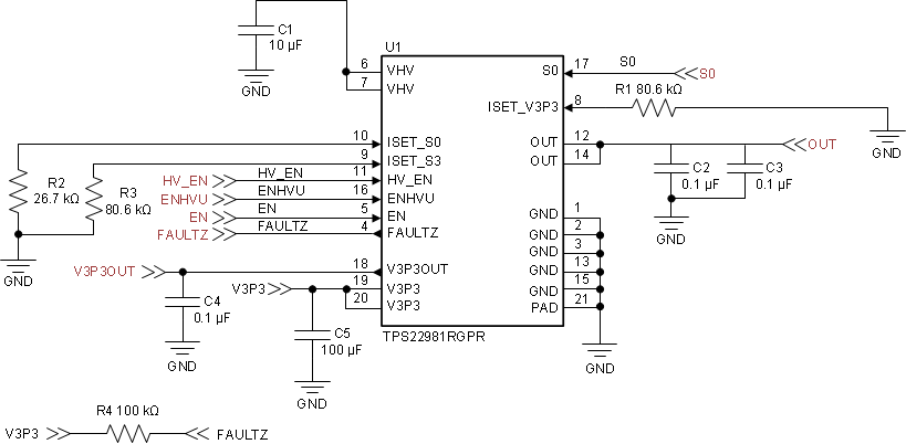 Figure 10. Layout Example Schematic
The TPS22981 can be placed on the same layer as its components. The layout can be a smaller area when the bottom is used for component placement. In this design example, the components and the TPS22981 are placed on the top layer. Figure 11 and Figure 12 show the suggested placement of the components.
For the nets V3P3, OUT, and VHV, TI recommends to use Thunderbolt three 8-mil or 16-mil vias when moving from layer to layer. A 40-mil trace or pour will allow roughly 2 A to pass current carrying capability with 0.5-oz. copper. Two 8-mil or 16-mil vias and 12-mil traces are sufficient for V3P3OUT. All of the other signals can be routed using a 10-mil trace with an 8-mil or 16-mil via. Figure 13 and Figure 14 show the suggested power and signal routing with and without a GND pour on the top layer. TI recommends that the capacitors and the GND pad on the TPS22981 are connected on the same plane.
The remaining signals can be routed through the bottom layer or other internal layer. Figure 15 shows the bottom routing.
10.2 Layout Example
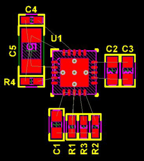 Figure 11. Top Layer 2D View
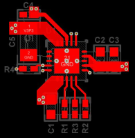 Figure 13. Power/Signal Routing
 Without GND Pour
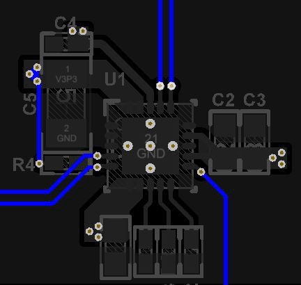 Figure 15. Bottom Layer Routing
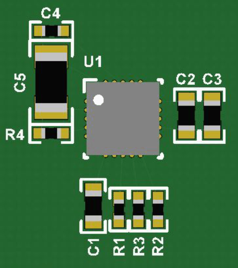 Figure 12. Top Layer 3D View
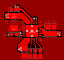 Figure 14. Power/Signal Routing
 With GND Pour