SLVSCL4B August 2014 – September 2014 TPS22994
PRODUCTION DATA.
- 1 Features
- 2 Applications
- 3 Description
- 4 Simplified Schematic
- 5 Revision History
- 6 Device Comparison Table
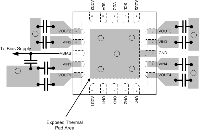
- 7 Pin Configuration and Functions
- 8 Specifications
-
9 Detailed Description
- 9.1 Overview
- 9.2 Functional Block Diagram
- 9.3
Feature Description
- 9.3.1 Operating Frequency
- 9.3.2 SDA/SCL Pin Configuration
- 9.3.3 Address (ADDx) Pin Configuration
- 9.3.4 On-Delay Control
- 9.3.5 Slew Rate Control
- 9.3.6 Quick Output Discharge (QOD) Control
- 9.3.7 Mode Registers
- 9.3.8 SwitchALL™ Command
- 9.3.9 VDD Supply For I2C Operation
- 9.3.10 Input Capacitor (Optional)
- 9.3.11 Output Capacitor (Optional)
- 9.3.12 I2C Protocol
- 9.4 Device Functional Modes
- 9.5 Register Map
-
10Applications and Implementation
- 10.1 Application Information
- 10.2 Typical Application
- 11Layout
- 12Device and Documentation Support
- 13Mechanical, Packaging, and Orderable Information
パッケージ・オプション
メカニカル・データ(パッケージ|ピン)
- RUK|20
サーマルパッド・メカニカル・データ
- RUK|20
発注情報
11 Layout
11.1 Board Layout
- VINx and VOUTx traces should be as short and wide as possible to accommodate for high current.
- Use vias under the exposed thermal pad for thermal relief for high current operation.
- The VINx terminals should be bypassed to ground with low ESR ceramic bypass capacitors. The typical recommended bypass capacitance is 1-µF ceramic with X5R or X7R dielectric. This capacitor should be placed as close to the device terminals as possible.
- The VOUTx terminals should be bypassed to ground with low ESR ceramic bypass capacitors. The typical recommended bypass capacitance is one-tenth of the VIN bypass capacitor of X5R or X7R dielectric rating. This capacitor should be placed as close to the device terminals as possible.
- The VBIAS terminal should be bypassed to ground with low ESR ceramic bypass capacitors. The typical recommended bypass capacitance is 0.1-µF ceramic with X5R or X7R dielectric.
- The VDD terminal should be bypassed to ground with low ESR ceramic bypass capacitors. The typical recommended bypass capacitance is 0.1-µF ceramic with X5R or X7R dielectric.
- ADDx pins should be tied high to VDD through a pull-up resistor or tied low to GND through a pull-down resistor.
The maximum IC junction temperature should be restricted to 125°C under normal operating conditions. To calculate the maximum allowable power dissipation, PD(max) for a given output current and ambient temperature, use the following equation:
Equation 4. 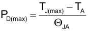
Where:
PD(max) = maximum allowable power dissipation
TJ(max) = maximum allowable junction temperature (125°C for the TPS22994)
TA = ambient temperature of the device
ΘJA = junction to air thermal impedance. See Thermal Information section. This parameter is highly dependent upon board layout.
The figure below shows an example of a layout.