JAJS365D January 2007 – October 2019 TPS2412 , TPS2413
PRODUCTION DATA.
- 1 特長
- 2 アプリケーション
- 3 概要
- 4 改訂履歴
- 5 概要(続き)
- 6 Device Comparison Table
- 7 Pin Configuration and Functions
- 8 Specifications
-
9 Detailed Description
- 9.1 Overview
- 9.2 Functional Block Diagram
- 9.3
Feature Description
- 9.3.1 Definitions
- 9.3.2 TPS2412 vs TPS2413 – MOSFET Control Methods
- 9.3.3 N+1 Power Supply – Typical Connection
- 9.3.4 Input ORing – Typical Connection
- 9.3.5 System Design and Behavior With Transients
- 9.3.6 TPS2412 Regulation-Loop Stability
- 9.3.7 MOSFET Selection and R(RSET)
- 9.3.8 Gate Drive, Charge Pump and C(BYP)
- 9.4 Device Functional Modes
- 10Application and Implementation
- 11Power Supply Recommendations
- 12Layout
- 13デバイスおよびドキュメントのサポート
- 14メカニカル、パッケージ、および注文情報
パッケージ・オプション
メカニカル・データ(パッケージ|ピン)
サーマルパッド・メカニカル・データ
発注情報
11.2 VDD, BYP, and Powering Options
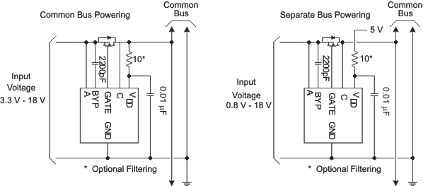
The separate VDD pin provides flexibility for operational power and controlled rail voltage. While the internal UVLO has been set to 2.5 V, the TPS2412/13 requires at least 3 V to generate the specified GATE drive voltage. Sufficient BYP voltage to run internal circuits occurs at VDD voltages from 2.5 V to 3 V. There are three choices for power, A, C, or a separate supply, two of which are demonstrated in Figure 14. One choice for voltage rails over 3.3 V is to power from C, because it is typically the source of reliable power. Voltage rails below 3.3 V nominal, for example, 2.5 V and below, should use a separate supply such as 5 V. A separate VDD supply can be used to control voltages above it, for example 5 V powering VDD to control a 12-V bus.
VDD is the main source of power for the internal control circuits. The charge pump that powers BYP draws most of its power from VDD. The input should be low impedance, making a bypass capacitor a preferred solution. A 10-Ω series resistor may be used to limit inrush current into the bypass capacitor, and to provide noise filtering for the supply.
BYP is the interconnection point between a charge pump, V(AC) monitor amplifiers and comparators, and the gate driver. C(BYP) must be used to filter the charge pump. A 2200 pF is recommended, but the value is not critical.
 Figure 14. VDD Powering Examples