SLVSCU5 March 2015 TPS25200-Q1
PRODUCTION DATA.
- 1 Features
- 2 Applications
- 3 Description
- 4 Simplified Schematic
- 5 Revision History
- 6 Pin Configuration and Functions
- 7 Specifications
- 8 Parameter Measurement Information
- 9 Detailed Description
- 10Application and Implementation
- 11Power Supply Recommendations
- 12Layout
- 13Device and Documentation Support
- 14Mechanical, Packaging, and Orderable Information
パッケージ・オプション
メカニカル・データ(パッケージ|ピン)
- DRV|6
サーマルパッド・メカニカル・データ
- DRV|6
発注情報
9 Detailed Description
9.1 Overview
The TPS25200-Q1 device is an intelligent low-voltage switch or e-Fuse with robust overcurrent and overvoltage protection which are suitable for a variety of applications.
The TPS25200-Q1 current-limited power switch uses N-channel MOSFETs in applications requiring up to 2.4 A of continuous load current. The device allows the user to program the current-limit threshold between 85 mA and 2.7 A (typical) through an external resistor. The device enters constant-current mode when the load exceeds the current-limit threshold.
The TPS25200-Q1 input can withstand 20-V DC voltage, but clamps VOUT to a precision regulated 5.4 V and shuts down in the event that the VIN value exceeds 7.6 V. The device also integrates overcurrent and short-circuit protection. The precision overcurrent limit helps minimize over designing of the input power supply while the fast response short-circuit protection isolates the load when a short circuit is detected.
The additional features of the device include the following:
- Overtemperature protection to safely shutdown in the event of an overcurrent event or a slight overvoltage event where the VOUT clamp is engaged over an extended period of time.
- Deglitched fault reporting to filter the FAULT signal to ensure that the TPS25200-Q1 device does not provide false-fault alerts.
- Output discharge pulldown to ensue a load is off and not in an undefined operational state.
- Reverse blocking when disabled to prevent back-drive from an active load which inadvertently causes undetermined behavior in the application.
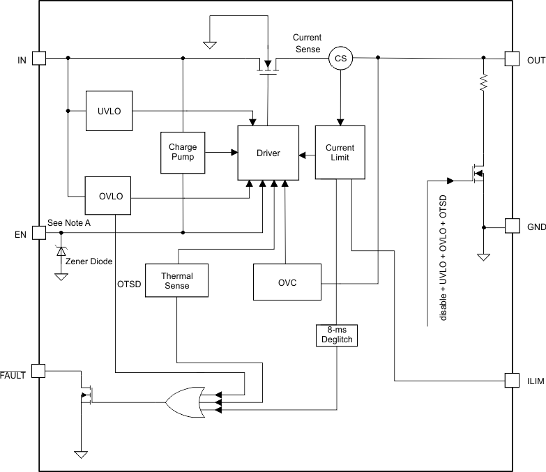
9.2 Functional Block Diagram

9.3 Feature Description
9.3.1 Enable
This logic enable input controls the power switch and device supply current. A logic-high input on the EN pin enables the driver, control circuits, and powers the switch. The enable input is compatible with both TTL and CMOS logic levels.
The EN pin can be tied to VIN with a pullup resistor, and is protected with an integrated Zener diode. Use a sufficiently large (300 kΩ) pullup resistor to ensure that V(EN) is limited below the absolute maximum rating.
9.3.2 Thermal Sense
The TPS25200-Q1 device uses two independent thermal sensing circuits for self protection that monitor the operating temperature of the power switch and disable operation if the temperature exceeds the values listed in the Recommended Operating Conditions table. The TPS25200-Q1 device operates in constant-current mode during an overcurrent condition, which increases the voltage drop across the power switch. The power dissipation in the package is proportional to the voltage drop across the power switch, which increases the junction temperature during an overcurrent condition. The first thermal sensor (OTSD1) turns off the power switch when the die temperature exceeds 135°C (minimum) and the device is in current-limit protection. Hysteresis is built into the thermal sensor, and the switch turns on after the device has cooled by approximately 20°C.
The TPS25200-Q1 device also has a second ambient thermal sensor (OTSD2). The thermal sensor turns off the power switch when the die temperature exceeds 155°C (minimum) regardless of whether the power switch is in current-limit protection and turns on the power switch after the device has cooled by approximately 20°C. The TPS25200-Q1 device continues to cycle off and on until the fault is removed.
9.3.3 Overcurrent Protection
The TPS25200-Q1 device initiates thermal protection by thermal cycling during an extended overcurrent condition. The device turns off when the junction temperature exceeds 135°C (typical) while in current limit. The device remains off until the junction temperature cools by 20°C (typical) and then restarts. The TPS25200-Q1 device cycles on and off until the overload is removed (see Figure 26 and Figure 29).
The TPS25200-Q1 device responds to an overcurrent condition by limiting the output current to the IOS levels shown in Figure 12. When an overcurrent condition is detected, the device maintains a constant output current and the output voltage is reduced accordingly. During an overcurrent event, two possible overload conditions can occur.
The first condition is when a short circuit or partial short circuit is present when the device is powered up or enabled. The output voltage is held near zero potential with respect to ground and the TPS25200-Q1 device ramps the output current to the IOS level. The TPS25200-Q1 device limits the current to the IOS level until the overload condition is removed or the device begins a thermal cycle.
The second condition is when a short circuit, partial short circuit, or transient overload occurs while the device is enabled and powered on. The device responds to the overcurrent condition within the time, tIOS (see Figure 12). The current-sense amplifier is overdriven during this time and momentarily disables the internal current-limit MOSFET. The current-sense amplifier recovers and limits the output current to the IOS level. Similar to the previous case, the TPS25200-Q1 device limits the current to the IOS level until the overload condition is removed or the device begins a thermal cycle.
9.3.4 FAULT Response
The FAULT open-drain output is asserted (active low) during an overcurrent, overtemperature, or overvoltage condition. The TPS25200-Q1 device asserts the FAULT signal until the fault condition is removed and the device resumes normal operation. The TPS25200-Q1 device is designed to eliminate false FAULT reporting by using an internal delay deglitch circuit for overcurrent (8-ms typical) conditions without the requirement for external circuitry. This design ensures that the FAULT signal is not accidentally asserted because of normal operation such as starting into a heavy capacitive load. The deglitch circuitry delays entering and leaving current-limit induced fault conditions.
The FAULT signal is not deglitched when the MOSFET is disabled because of an overtemperature condition but is deglitched after the device has cooled and begins to turn on. This unidirectional deglitch prevents FAULT oscillation during an overtemperature event.
The FAULT signal is not deglitched when the MOSFET is disabled into overvoltage-lockout (OVLO) or out of OVLO. The TPS25200-Q1 device does not assert the FAULT during output-voltage clamp mode.
Connect the FAULT pin with a pullup resistor to a low-voltage I/O rail.
9.3.5 Output Discharge
A 480-Ω (typical) output discharge dissipates the stored charge and leakage current on the OUT pin when the TPS25200-Q1 device is in undervoltage-lockout (UVLO) or OVLO or is disabled. The pulldown capability decreases as VIN decreases (see Figure 8).
9.4 Device Functional Modes
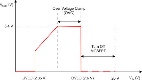
The input voltage of the TPS25200-Q1 device can withstand up to 20 V. The input voltage, within a range of 0 V to 20 V, can be divided to four modes which are described in the following sections.
 Figure 13. Output vs Input Voltage
9.4.1 Undervoltage Lockout (UVLO)
The undervoltage lockout (UVLO) circuit disables the power switch until the input voltage reaches the UVLO turn-on threshold. Built-in hysteresis prevents unwanted on and off cycling because of input voltage droop during turn on.
9.4.2 Overcurrent Protection (OCP)
When 2.35 V < VIN < 5.4 V, the TPS25200-Q1 device is a traditional power switch that provides overcurrent protection.
9.4.3 Overvoltage Clamp (OVC)
When 5.4 V < VIN < 7.6 V, the overvoltage-clamp (OVC) circuit clamps the output voltage to 5.4 V. Within this VIN range, the overcurrent protection remains active. Fast transients can exceed the bandwidth of the internal gate-control amplifier but such events will not risk damage to the load. In the unlikely event that a transient is fast enough to exceed the amplifier bandwidth but not severe enough to exceed 7.6 V, it may cause momentary droops in VOUT while the amplifier catches up and settles on VOUT = 5.4 V. For example, a 5-V to 7-V transient with 0.5-V/ms slew rate and with 2 × 47 µF // 100-Ω load, some drooping occurs at VOUT.
9.4.4 Overvoltage Lockout (OVLO)
When VIN exceeds 7.6 V, the overvoltage lockout (OVLO) circuit turns off the protected power switch.