JAJSK66A March   2021  – March 2022 TPS2521

PRODUCTION DATA  

  1. 特長
  2. アプリケーション
  3. 概要
  4. Revision History
  5. Device Comparison Table
  6. Pin Configuration and Functions
  7. Specifications
    1. 7.1 Absolute Maximum Ratings
    2. 7.2 ESD Ratings
    3. 7.3 Recommended Operating Conditions
    4. 7.4 Thermal Information
    5. 7.5 Electrical Characteristics
    6. 7.6 Timing Requirements
    7. 7.7 Switching Characteristics
      1.      15
    8. 7.8 Typical Characteristics
  8. Detailed Description
    1. 8.1 Overview
    2. 8.2 Functional Block Diagram
    3. 8.3 Feature Description
      1. 8.3.1 Input Reverse Polarity Protection
      2. 8.3.2 Undervoltage Lockout (UVLO and UVP)
      3. 8.3.3 Overvoltage Clamp (OVC)
      4. 8.3.4 Inrush Current, Overcurrent, and Short Circuit Protection
        1. 8.3.4.1 Slew Rate (dVdt) and Inrush Current Control
        2. 8.3.4.2 Active Current Limiting
        3. 8.3.4.3 Short-Circuit Protection
      5. 8.3.5 Analog Load Current Monitor
      6. 8.3.6 Reverse Current Protection
      7. 8.3.7 Overtemperature Protection (OTP)
      8. 8.3.8 Fault Response
      9. 8.3.9 Power Good Indication (PG)
    4. 8.4 Device Functional Modes
  9. Application and Implementation
    1. 9.1 Application Information
    2. 9.2 Single Device, Self-Controlled
    3. 9.3 Typical Application
      1. 9.3.1 Application
      2. 9.3.2 Design Requirements
      3. 9.3.3 Detailed Design Procedure
        1. 9.3.3.1 Device Selection
        2. 9.3.3.2 Setting Undervoltage and Overvoltage Thresholds
        3. 9.3.3.3 Setting Output Voltage Rise Time (tR)
        4. 9.3.3.4 Setting Power Good Assertion Threshold
        5. 9.3.3.5 Setting Overcurrent Threshold (ILIM)
        6. 9.3.3.6 Setting Overcurrent Blanking Interval (tITIMER)
      4. 9.3.4 Application Curves
  10. 10Power Supply Recommendations
    1. 10.1 Transient Protection
    2. 10.2 Output Short-Circuit Measurements
  11. 11Layout
    1. 11.1 Layout Guidelines
    2. 11.2 Layout Example
  12. 12Device and Documentation Support
    1. 12.1 Documentation Support
      1. 12.1.1 Related Documentation
    2. 12.2 Receiving Notification of Documentation Updates
    3. 12.3 サポート・リソース
    4. 12.4 Trademarks
    5. 12.5 Electrostatic Discharge Caution
    6. 12.6 Glossary
  13. 13Mechanical, Packaging, and Orderable Information

パッケージ・オプション

メカニカル・データ(パッケージ|ピン)
サーマルパッド・メカニカル・データ
発注情報

Setting Output Voltage Rise Time (tR)

The slew rate (SR) needed to meet the target specification is:

Equation 8. GUID-20210324-CA0I-3GJK-JKW6-BQZHXHCGQQCM-low.gif

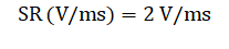
The CdVdt needed to achieve this slew rate can be calculated as:

Equation 9. GUID-20210324-CA0I-59RQ-20PP-S7BBVT8NQ3T8-low.gif

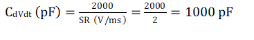
Choose the nearest standard capacitor value as 1 nF.

For this slew rate, the inrush current can be calculated as:

Equation 10. GUID-20210324-CA0I-0JTQ-4BNC-ZQBJ9KVHXLSB-low.gif

The average power dissipation inside the part during inrush can be calculated as:

Equation 11. GUID-20210324-CA0I-VDGF-DGTJ-CCNW2XKMM0D4-low.gif

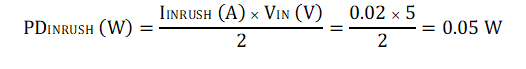
The power dissipation is below the allowed limit for a successful start-up without hitting thermal shut-down within the target rise time as shown in Figure 9-4.

Figure 9-4 Thermal Shut-Down Plot During Inrush