JAJSCJ7 September   2016 TPS2549

PRODUCTION DATA.  

  1. 特長
  2. アプリケーション
  3. 概要
  4. 改訂履歴
  5. Pin Configuration and Functions
  6. Specifications
    1. 6.1 Absolute Maximum Ratings
    2. 6.2 ESD Ratings
    3. 6.3 Recommended Operating Conditions
    4. 6.4 Thermal Information
    5. 6.5 Electrical Characteristics
    6. 6.6 Switching Characteristics
    7. 6.7 Typical Characteristics
  7. Parameter Measurement Information
  8. Detailed Description
    1. 8.1 Overview
    2. 8.2 Functional Block Diagram
    3. 8.3 Feature Description
      1. 8.3.1  FAULT Response
      2. 8.3.2  Cable Compensation
        1. 8.3.2.1 Design Procedure
      3. 8.3.3  D+ and D- Protection
      4. 8.3.4  Output and D+ or D- Discharge
      5. 8.3.5  Port Power Management (PPM)
        1. 8.3.5.1 Benefits of PPM
        2. 8.3.5.2 PPM Details
        3. 8.3.5.3 Implementing PPM in a System With Two Charging Ports (CDP and SDP1)
        4. 8.3.5.4 Implementing PPM in a System With Two Charging Ports (DCP and DCP1)
      6. 8.3.6  CDP and SDP Auto Switch
      7. 8.3.7  Overcurrent Protection
      8. 8.3.8  Undervoltage Lockout
      9. 8.3.9  Thermal Sensing
      10. 8.3.10 Current Limit Setting
    4. 8.4 Device Functional Modes
      1. 8.4.1 Device Truth Table (TT)
      2. 8.4.2 USB Specification Overview
      3. 8.4.3 Standard Downstream Port (SDP) Mode — USB 2.0 and USB 3.0
      4. 8.4.4 Charging Downstream Port (CDP) Mode
      5. 8.4.5 Dedicated Charging Port (DCP) Mode
        1. 8.4.5.1 DCP BC1.2 and YD/T 1591-2009
        2. 8.4.5.2 DCP Divider-Charging Scheme
        3. 8.4.5.3 DCP 1.2-V Charging Scheme
      6. 8.4.6 DCP Auto Mode
      7. 8.4.7 Client Mode
      8. 8.4.8 High-Bandwidth Data-Line Switches
  9. Application and Implementation
    1. 9.1 Application Information
    2. 9.2 Typical Application
      1. 9.2.1 Design Requirements
      2. 9.2.2 Detailed Design Procedure
        1. 9.2.2.1 Input and Output Capacitance
        2. 9.2.2.2 Cable Compensation Calculation
        3. 9.2.2.3 Power Dissipation and Junction Temperature
      3. 9.2.3 Application Curves
  10. 10Power Supply Recommendations
  11. 11Layout
    1. 11.1 Layout Guidelines
    2. 11.2 Layout Example
  12. 12デバイスおよびドキュメントのサポート
    1. 12.1 ドキュメントのサポート
      1. 12.1.1 関連資料
    2. 12.2 ドキュメントの更新通知を受け取る方法
    3. 12.3 コミュニティ・リソース
    4. 12.4 商標
    5. 12.5 静電気放電に関する注意事項
    6. 12.6 Glossary
  13. 13メカニカル、パッケージ、および注文情報

パッケージ・オプション

メカニカル・データ(パッケージ|ピン)
サーマルパッド・メカニカル・データ
発注情報

Layout

Layout Guidelines

  • For the trace routing of DP_IN, DM_IN, DP_OUT, and DM_OUT: Route these traces as micro-strips with nominal differential impedance of 90 Ω. Minimize the use of vias in the high-speed data lines. Keep the reference GND plane devoid from cuts or splits above the differential pairs to prevent impedance discontinuities. For more information, see the High Speed USB Platform Design Guideline from Intel.
  • The trace routing from the upstream regulator to the TPS2549 IN pin should as short as possible to reduce the voltage drop and parasitic inductance.
  • The traces routing from the RILIM_HI and RILIM_LO resistors to the device should be as short as possible to reduce parasitic effects on the current-limit accuracy.
  • The thermal pad should be directly connected to the PCB ground plane using a wide and short copper trace.
  • The trace routing from the CS pin to the feedback divider of the upstream regulator should not be routed near any noise sources that can capacitively couple to the feedback divider.

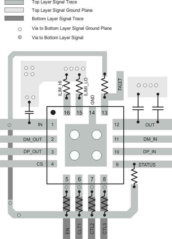
Layout Example

TPS2549 layout_SLUSCE3.gif Figure 58. TPS2549 Layout Diagram