SLVSCR1C September 2015 – July 2017 TPS25810
PRODUCTION DATA.
- 1 Features
- 2 Applications
- 3 Description
- 4 Revision History
- 5 Pin Configuration and Functions
- 6 Specifications
-
7 Detailed Description
- 7.1 Overview
- 7.2 Functional Block Diagram
- 7.3
Feature Description
- 7.3.1 Configuration Channel Pins CC1 and CC2
- 7.3.2 Current Capability Advertisement and Overload Protection
- 7.3.3
Undervoltage Lockout (UVLO)
- 7.3.3.1 Device Power Pins (IN1, IN2, AUX, OUT, and GND)
- 7.3.3.2 FAULT Response
- 7.3.3.3 Thermal Shutdown
- 7.3.3.4 REF
- 7.3.3.5 Audio Accessory Detection
- 7.3.3.6 Debug Accessory Detection
- 7.3.3.7 Plug Polarity Detection
- 7.3.3.8 Device Enable Control
- 7.3.3.9 Load Detect
- 7.3.3.10 Power Wake
- 7.3.3.11 Port Power Management (PPM)
- 7.3.3.12 Implementing PPM in a System with Two Type-C Ports
- 7.3.3.13 PPM Operation
- 7.4 Device Functional Modes
- 8 Application and Implementation
- 9 Power Supply Recommendations
- 10Layout
- 11Device and Documentation Support
- 12Mechanical, Packaging, and Orderable Information
パッケージ・オプション
メカニカル・データ(パッケージ|ピン)
- RVC|20
サーマルパッド・メカニカル・データ
- RVC|20
発注情報
8 Application and Implementation
NOTE
Information in the following applications sections is not part of the TI component specification, and TI does not warrant its accuracy or completeness. TI’s customers are responsible for determining suitability of components for their purposes. Customers should validate and test their design implementation to confirm system functionality.
8.1 Application Information
The TPS25810 is a Type-C DFP controller that supports all Type-C DFP required functions. The TPS25810 only applies power to VBUS when it detects that a UFP is attached and removes power when it detects the UFP is detached. The device exposes its identity via its CC pin advertising its current capability based on CHG and CHG_HI pin settings. The TPS25810 also limits its advertised current internally and provides robust protection to a fault on the system VBUS power rail.
After a connection is established by the TPS25810, the device is capable of providing VCONN to power circuits in the cable plug on the CC pin that is not connected to the CC wire in the cable. VCONN is internally current limited and has its own supply pin IN2. Apart from providing charging current to a UFP, the TPS25810 also supports Audio and Debug accessory modes.
The following design procedure can be used to implement a full featured Type-C DFP.
NOTE
BC 1.2 is not supported in the TPS25810. To support BC1.2 with Type-C charging modes in a single C connector, a device like a TPS2514A will need to be used.
8.2 Typical Applications
8.2.1 Type C DFP Port Implementation without BC 1.2 Support
Figure 20 shows a minimal Type-C DFP implementation capable of supporting 5-V and 3-A charging.
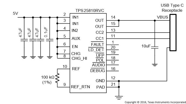 Figure 20. Type-C DFP Port Implementation without BC 1.2 Support
8.2.1.1 Design Requirements
8.2.1.1.1 Input and Output Capacitance
Input and output capacitance improves the performance of the device. The actual capacitance should be optimized for the particular application. For all applications, a 0.1-μF or greater ceramic bypass capacitor between IN and GND is recommended as close to the device as possible for local noise de-coupling.
All protection circuits such as the TPS25810 have the potential for input voltage overshoots and output voltage undershoots. Input voltage overshoots can be caused by either of two effects. The first cause is an abrupt application of input voltage in conjunction with input power bus inductance and input capacitance when the IN terminal is high impedance (before turn on). Theoretically, the peak voltage is 2 times the applied. The second cause is due to the abrupt reduction of output short circuit current when the TPS25810 turns off and energy stored in the input inductance drives the input voltage high. Input voltage droops may also occur with large load steps and as the TPS25810 output is shorted. Applications with large input inductance (for instance connecting the evaluation board to the bench power-supply through long cables) may require large input capacitance to reduce the voltage overshoot from exceeding the absolute maximum voltage of the device.
The fast current-limit speed of the TPS25810 to hard output short circuits isolate the input bus form faults. However, ceramic input capacitance in the range of 1 μF to 22 μF adjacent to the TPS25810 input aids in both response time and limiting the transient seen on the input power bus. Momentary input transients to 6.5 V are permitted. Output voltage undershoot is caused by the inductance of the output power bus just after a short has occurred and the TPS25810 has abruptly reduced OUT current. Energy stored in the inductance drives the OUT voltage down and potentially negative as it discharges. An application with large output inductance (such as from a cable) benefits from use of a high-value output capacitor to control voltage undershoot.
When implementing a USB standard application, 120 μF minimum output capacitance is required. Typically a 150-μF electrolytic capacitor is used, which is sufficient to control voltage undershoots. Since in Type-C DFP is a cold socket when no UFP is attached, the output capacitance should be placed at the IN pin versus OUT as is used in USB Type A ports. It is also recommended to put a 10-μF ceramic capacitor on the OUT pin for better voltage bypass.
8.2.1.2 Detailed Design Procedure
The TPS25810 device supports three different input voltages based on the application. In the simplest implementation all input supplies are tied to a single voltage source as shown in Figure 20 which is set to 5 V. However, it is recommended to set a slightly higher (100 mV to 200 mV) input voltage, when possible, to compensate for IR drop from the source to the Type C connector.
Other design considerations are listed below:
- Place at least 120 µF of bypass capacitance close to the IN pins versus OUT as Type C is a cold socket connector.
- A 10-µF bypass capacitor is recommended placed near a Type-C receptacle VBUS pin to handle load transients.
- Depending on the max current level advertisement supported by the Type-C port in the system, set CHG and CHG_HI levels accordingly. 3 A advertisement is shown in Figure 20.
- EN, CHG, and CHG_HI pins can be tied directly to GND or VAUX without a pull-up resistor.
- CHG and CHG_HI can also be dynamically controlled by a µC to change the current advertisement level to the UFP.
- When an open drain output of the TPS25810 is not used, it can be left as NC or tied to GND.
- Use a 1% 100-kΩ resistor to connect between the REF and REF_RTN pins placing it close to the device pin and isolated from switching noise on the board.
8.2.1.3 Application Curves
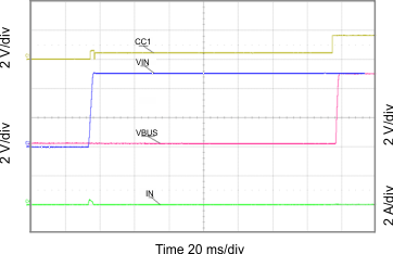
| Basic Start-Up: IN1 = IN2 = AUX = EN = CHG = CHG_HI = 5 V, CC1 = Rd, CC2 = Open | ||
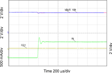
| IN1 = IN2 = AUX = EN = 5 V; CHG = CHG_HI = 0 V, CC1 = Open, CC2 = Rd, OUT = Open→5 Ω | ||
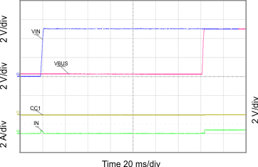
| IN1 = IN2 = AUX = EN = CHG = CHG_HI = 5 V, CC1 = Short, CC2 = Rd | ||
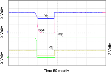
| VIN 5 V→3.5 V (100 ms)→5 V (1 V/ms), | ||||
| IN1 = IN2 = AUX = EN = CHG = CHG_HI = 5 V, | ||||
| CC1 = Rd, CC2 = Ra | ||||
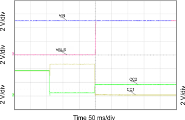
| IN1 = IN2 = AUX = EN = CHG = CHG_HI = 5 V, CC1 = Open, CC2 = Open then Rd | ||
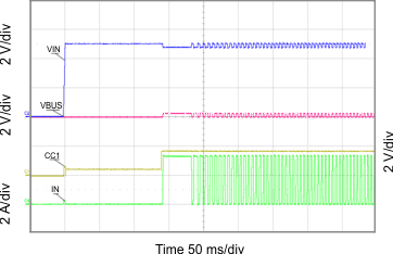
| IN1 = IN2 = AUX = EN = CHG = CHG_HI = 5 V, CC1 = Rd, CC2 = Open, OUT = Shorted | ||
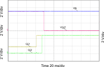
| IN1 = IN2 = AUX = EN = CHG = CHG_HI = 5 V, CC1 = Open, CC2 = Rd→Open | ||
8.2.2 Type-C DFP Port Implementation with BC 1.2 (DCP Mode) Support
Figure 28 shows a Type-C DFP implementation capable of supporting 5 V and 3 A charging in a Type-C port that is also able to support charging of legacy devices when used with a Type C – µB cable assembly for charging phones and handheld devices equipped with µB connector.
This implementation requires the use of a TPS2514A, a USB dedicated charging port (DCP) controller with auto-detect feature to charge not only BC1.2 compliant handheld devices but also popular phones and tablets that incorporate their own propriety charging algorithm. Refer to TPS2514A specifications available at www.ti.com for more details.
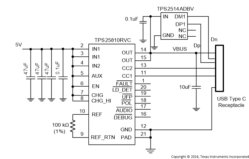 Figure 28. Type C DFP Port Implementation with BC 1.2 (DCP Mode) Support
8.2.2.1 Design Requirements
Refer to Design Requirements for the Design Requirements.
8.2.2.2 Detailed Design Procedure
Refer to Detailed Design Procedure for the Detailed Design Procedure.
8.2.2.3 Application Curves
Refer to Application Curves for the Application Curves.