JAJSMR0 August 2021 TPS25860-Q1 , TPS25862-Q1
PRODUCTION DATA
- 1 特長
- 2 アプリケーション
- 3 概要
- 4 Revision History
- 5 概要 (続き)
- 6 Device Comparison Table
- 7 Pin Configuration and Functions
- 8 Specifications
- 9 Parameter Measurement Information
-
10Detailed Description
- 10.1 Overview
- 10.2 Functional Block Diagram
- 10.3
Feature Description
- 10.3.1 Power-Down or Undervoltage Lockout
- 10.3.2 Input Overvoltage Protection (OVP) - Continuously Monitored
- 10.3.3 Buck Converter
- 10.3.4 FREQ/SYNC
- 10.3.5 Bootstrap Voltage (BOOT)
- 10.3.6 Minimum ON-Time, Minimum OFF-Time
- 10.3.7 Internal Compensation
- 10.3.8 Selectable Output Voltage (VSET)
- 10.3.9 Current Limit and Short Circuit Protection
- 10.3.10 Cable Compensation
- 10.3.11 Thermal Management with Temperature Sensing (TS) and OTSD
- 10.3.12 Thermal Shutdown
- 10.3.13 USB Enable On/Off Control (TPS25862-Q1)
- 10.3.14 FAULT Indication
- 10.3.15 USB Specification Overview
- 10.3.16 USB Type-C® Basics
- 10.3.17 USB Port Operating Modes
- 10.4 Device Functional Modes
-
11Application and Implementation
- 11.1 Application Information
- 11.2
Typical Applications
- 11.2.1 Design Requirements
- 11.2.2
Detailed Design Procedure
- 11.2.2.1 Output Voltage Setting
- 11.2.2.2 Switching Frequency
- 11.2.2.3 Inductor Selection
- 11.2.2.4 Output Capacitor Selection
- 11.2.2.5 Input Capacitor Selection
- 11.2.2.6 Bootstrap Capacitor Selection
- 11.2.2.7 Undervoltage Lockout Set-Point
- 11.2.2.8 Cable Compensation Set-Point
- 11.2.2.9 FAULT Resistor Selection
- 11.2.3 Application Curves
- 12Power Supply Recommendations
- 13Layout
- 14Device and Documentation Support
- 15Mechanical, Packaging, and Orderable Information
10.3.6 Minimum ON-Time, Minimum OFF-Time
Minimum ON-time, TON_MIN, is the smallest duration of time that the HS switch can be on. TON_MIN is typically 84 ns in the TPS2586x-Q1. Minimum OFF-time, TOFF_MIN, is the smallest duration that the HS switch can be off. TOFF_MIN is typically 81 ns in the TPS2586x-Q1. In CCM (FPWM) operation, TON_MIN and TOFF_MIN limit the voltage conversion range given in a selected switching frequency.
The minimum duty cycle allowed is:
And the maximum duty cycle allowed is:
Given fixed TON_MIN and TOFF_MIN, the higher the switching frequency, the narrower the range of the allowed duty cycle.
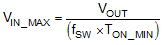
Given an output voltage, the choice of the switching frequency affects the allowed input voltage range, solution size, and efficiency. The maximum operation supply voltage can be found by:
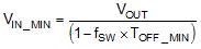
At lower supply voltage, the switching frequency is limited by TOFF_MIN. The minimum VIN can be approximated by:
Considering power losses in the system with heavy load operation, VIN_MAX is higher than the result calculated in Equation 7.
If minimum ON-time or minimum OFF-time do not support the desired conversion ratio, frequency is reduced, automatically allowing regulation to be maintained during load dump and with very low dropout during cold crank even with high operating-frequency setting.