JAJSMF6C november   2021  – april 2023 TPS2597

PRODUCTION DATA  

  1. 特長
  2. アプリケーション
  3. 概要
  4. Revision History
  5. Device Comparison Table
  6. Pin Configuration and Functions
  7. Specifications
    1. 7.1 Absolute Maximum Ratings
    2. 7.2 ESD Ratings
    3. 7.3 Recommended Operating Conditions
    4. 7.4 Thermal Information
    5. 7.5 Electrical Characteristics
    6. 7.6 Timing Requirements
    7. 7.7 Switching Characteristics
    8. 7.8 Typical Characteristics
  8. Detailed Description
    1. 8.1 Overview
    2. 8.2 Functional Block Diagram
    3. 8.3 Feature Description
      1. 8.3.1 Undervoltage Lockout (UVLO and UVP)
      2. 8.3.2 Overvoltage Lockout (OVLO)
      3. 8.3.3 Overvoltage Clamp (OVC)
      4. 8.3.4 Inrush Current, Overcurrent, and Short Circuit Protection
        1. 8.3.4.1 Slew Rate (dVdt) and Inrush Current Control
        2. 8.3.4.2 Circuit-Breaker
        3. 8.3.4.3 Active Current Limiting
        4. 8.3.4.4 Short-Circuit Protection
      5. 8.3.5 Analog Load Current Monitor
      6. 8.3.6 Overtemperature Protection (OTP)
      7. 8.3.7 Fault Response and Indication (FLT)
      8. 8.3.8 Power-Good Indication (PG)
    4. 8.4 Device Functional Modes
  9. Application and Implementation
    1. 9.1 Application Information
      1. 9.1.1 Single Device, Self-Controlled
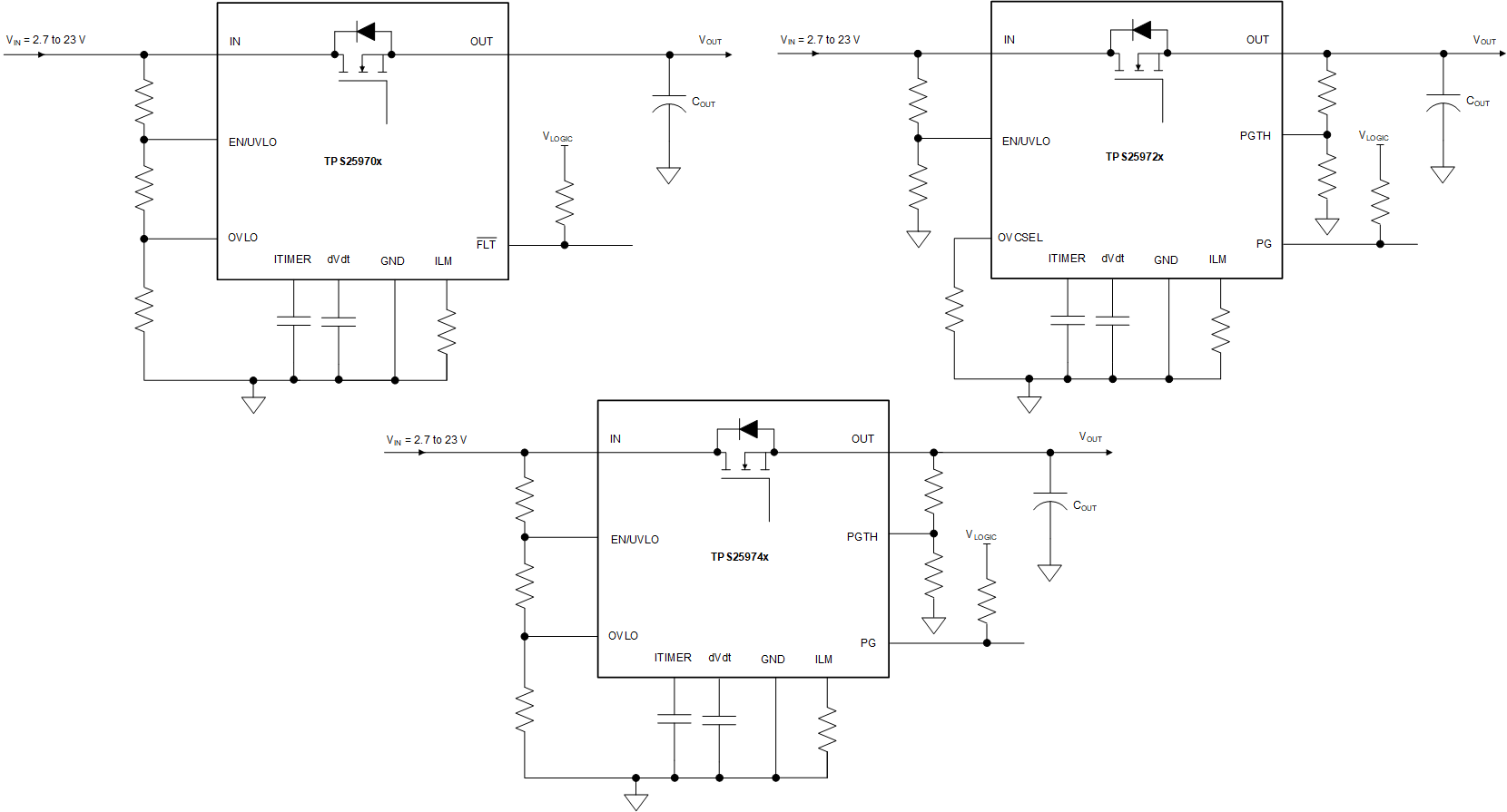
    2. 9.2 Typical Application
      1. 9.2.1 Design Requirements
      2. 9.2.2 Detailed Design Procedure
        1. 9.2.2.1 Device Selection
        2. 9.2.2.2 Setting Undervoltage and Overvoltage Thresholds
        3. 9.2.2.3 Setting Output Voltage Rise Time (tR)
        4. 9.2.2.4 Setting Power-Good Assertion Threshold
        5. 9.2.2.5 Setting Overcurrent Threshold (ILIM)
        6. 9.2.2.6 Setting Overcurrent Blanking Interval (tITIMER)
      3. 9.2.3 Application Curves
    3. 9.3 Parallel Operation
    4. 9.4 Power Supply Recommendations
      1. 9.4.1 Transient Protection
      2. 9.4.2 Output Short-Circuit Measurements
    5. 9.5 Layout
      1. 9.5.1 Layout Guidelines
      2. 9.5.2 Layout Example
  10. 10Device and Documentation Support
    1. 10.1 Device Support
      1. 10.1.1 サード・パーティ製品に関する免責事項
    2. 10.2 Documentation Support
      1. 10.2.1 Related Documentation
    3. 10.3 ドキュメントの更新通知を受け取る方法
    4. 10.4 サポート・リソース
    5. 10.5 Trademarks
    6. 10.6 静電気放電に関する注意事項
    7. 10.7 用語集
  11. 11Mechanical, Packaging, and Orderable Information

パッケージ・オプション

メカニカル・データ(パッケージ|ピン)
サーマルパッド・メカニカル・データ
発注情報

Single Device, Self-Controlled

GUID-20211025-SS0I-2D5D-VWGP-FZVH3FPW5CFJ-low.gif

Figure 9-1 Single Device, Self-Controlled

Other variations:

In a Host MCU controlled system, EN/UVLO or OVLO can also be driven from the host GPIO to control the device.

ILM pin can be connected to the MCU ADC input for current monitoring purpose.

Note:

TI recommends to keep parasitic capacitance on ILM pin below 50 pF to ensure stable operation.

For the TPS25972x and TPS25974x variants, either VIN or VOUT can be used to drive the PGTH resistor divider depending on which supply must be monitored for Power Good indication.