JAJSJ14 August 2020 TPS25980
PRODUCTION DATA
- 1 特長
- 2 アプリケーション
- 3 概要
- 4 Revision History
- 5 Device Comparison Table
- 6 Pin Configuration and Functions
- 7 Specifications
-
8 Detailed Description
- 8.1 Overview
- 8.2 Functional Block Diagram
- 8.3 Feature Description
- 8.4 Fault Response
- 8.5 Device Functional Modes
-
9 Application and Implementation
- 9.1 Application Information
- 9.2
Typical Application: Patient Monitoring System in Medical Applications
- 9.2.1 Design Requirements
- 9.2.2
Detailed Design Procedure
- 9.2.2.1 Device Selection
- 9.2.2.2 Setting the Current Limit Threshold: RILIM Selection
- 9.2.2.3 Setting the Undervoltage Lockout Set Point
- 9.2.2.4 Choosing the Current Monitoring Resistor: RIMON
- 9.2.2.5 Setting the Output Voltage Ramp Time (TdVdt)
- 9.2.2.6 Setting the Load Handshake (LDSTRT) Delay
- 9.2.2.7 Setting the Transient Overcurrent Blanking Interval (tITIMER)
- 9.2.2.8 Setting the Auto-Retry Delay and Number of Retries
- 9.2.3 Application Curves
- 9.3 System Examples
- 10Power Supply Recommendations
- 11Layout
- 12Device and Documentation Support
- 13Mechanical, Packaging, and Orderable Information
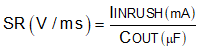
8.3.3.1 Slew Rate and Inrush Current Control (dVdt)
During hot-plug events or while trying to charge a large output capacitance, there can be a large inrush current. If the inrush current is not controlled, it can damage the input connectors and/or cause the system power supply to droop leading to unexpected restarts elsewhere in the system. The TPS25980x provides integrated output slew rate (dVdt) control to manage the inrush current during start-up. The inrush current is directly proportional to the load capacitance and rising slew rate. The following equation can be used to calculate the slew rate (SR) required to limit the inrush current (IINRUSH) for a given load capacitance (COUT):
An external capacitance can be connected to the dVdt pin to control the rising slew rate and lower the inrush current during turn on. The required CdVdt capacitance to produce a given slew rate can be calculated using the following formula:
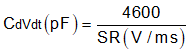
The fastest output slew rate is achieved by leaving the dVdt pin open.