JAJSHA8A February   2018  – April 2019 TPS2HB50-Q1

ADVANCE INFORMATION for pre-production products; subject to change without notice.  

  1. 特長
  2. アプリケーション
  3. 概要
    1.     概略回路図
  4. 改訂履歴
  5. Device Comparison Table
  6. Pin Configuration and Functions
    1.     Pin Functions
    2. 6.1 Recommended Connections for Unused Pins
  7. Specifications
    1. Table 3. Absolute Maximum Ratings
    2. Table 4. ESD Ratings
    3. Table 5. Recommended Operating Conditions
    4. Table 6. Thermal Information
    5. Table 7. Electrical Characteristics
    6. Table 8. SNS Timing Characteristics
    7. Table 9. Switching Characteristics
  8. Parameter Measurement Information
  9. Detailed Description
    1. 9.1 Overview
    2. 9.2 Functional Block Diagram
    3. 9.3 Feature Description
      1. 9.3.1 Protection Mechanisms
        1. 9.3.1.1 Thermal Shutdown
        2. 9.3.1.2 Current Limit
          1. 9.3.1.2.1 Current Limit Foldback
          2. 9.3.1.2.2 Programmable Current Limit
          3. 9.3.1.2.3 Undervoltage Lockout (UVLO)
          4. 9.3.1.2.4 VBB During Short-to-Ground
        3. 9.3.1.3 Voltage Transients
          1. 9.3.1.3.1 Load Dump
        4. 9.3.1.4 Driving Inductive Loads
        5. 9.3.1.5 Reverse Battery
        6. 9.3.1.6 Fault Event – Timing Diagrams
      2. 9.3.2 Diagnostic Mechanisms
        1. 9.3.2.1 VOUTx Short-to-Battery and Open-Load
          1. 9.3.2.1.1 Detection With Switch Enabled
          2. 9.3.2.1.2 Detection With Switch Disabled
        2. 9.3.2.2 SNS Output
          1. 9.3.2.2.1 RSNS Value
            1. 9.3.2.2.1.1 High Accuracy Load Current Sense
            2. 9.3.2.2.1.2 SNS Output Filter
        3. 9.3.2.3 Fault Indication and SNS Mux
        4. 9.3.2.4 Resistor Sharing
        5. 9.3.2.5 High-Frequency, Low Duty-Cycle Current Sensing
    4. 9.4 Device Functional Modes
      1. 9.4.1 Off
      2. 9.4.2 Standby
      3. 9.4.3 Diagnostic
      4. 9.4.4 Standby Delay
      5. 9.4.5 Active
      6. 9.4.6 Fault
  10. 10Application and Implementation
    1. 10.1 Application Information
      1. 10.1.1 Ground Protection Network
      2. 10.1.2 Interface With Microcontroller
      3. 10.1.3 I/O Protection
      4. 10.1.4 Inverse Current
      5. 10.1.5 Loss of GND
      6. 10.1.6 Automotive Standards
        1. 10.1.6.1 ISO7637-2
        2. 10.1.6.2 AEC – Q100-012 Short Circuit Reliability
    2. 10.2 Typical Application
      1. 10.2.1 Design Requirements
      2. 10.2.2 Detailed Design Procedure
        1. 10.2.2.1 Thermal Considerations
        2. 10.2.2.2 RILIM Calculation
        3. 10.2.2.3 Diagnostics
          1. 10.2.2.3.1 Selecting the RSNS Value
  11. 11Power Supply Recommendations
  12. 12Layout
    1. 12.1 Layout Guidelines
    2. 12.2 Layout Example
  13. 13デバイスおよびドキュメントのサポート
    1. 13.1 ドキュメントのサポート
      1. 13.1.1 関連資料
    2. 13.2 ドキュメントの更新通知を受け取る方法
    3. 13.3 コミュニティ・リソース
    4. 13.4 商標
    5. 13.5 静電気放電に関する注意事項
    6. 13.6 Glossary
  14. 14メカニカル、パッケージ、および注文情報

パッケージ・オプション

メカニカル・データ(パッケージ|ピン)
サーマルパッド・メカニカル・データ
発注情報

Typical Application

This application example demonstrates how the TPS2HB50-Q1 device can be used to power resistive heater loads in automotive seats. In this example, we consider dual heater loads that are powered independently by the two channels of the device. A dual-channel device is the ideal solution as it will yield a smaller solution size relative to two single-channel devices.
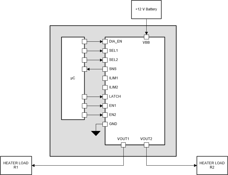
TPS2HB50-Q1 Typical_App_Heater_SLVSDZ3.gifFigure 16. Block Diagram for Powering Dual Heater Loads