JAJSQ83F november 1998 – october 2020
PRODUCTION DATA
- 1
- 1 特長
- 2 アプリケーション
- 3 概要
- 4 Revision History
- 5 Device Comparison Table
- 6 Pin Configuration and Functions
-
7 Specifications
- 7.1 Absolute Maximum Ratings
- 7.2 ESD Ratings
- 7.3 Recommended Operating Conditions
- 7.4 Thermal Information
- 7.5 Electrical Characteristics
- 7.6 Electrical Characteristics for TPS3705-33 Only
- 7.7 Timing Requirements
- 7.8 Switching Characteristics
- 7.9 Dissipation Ratings
- 7.10 Timing Diagram
- 7.11 Typical Characteristics
- 8 Detailed Description
- 9 Application and Implementation
- 10Power Supply Recommendations
- 11Layout
- 12Device and Documentation Support
- 13Mechanical, Packaging, and Orderable Information
パッケージ・オプション
メカニカル・データ(パッケージ|ピン)
サーマルパッド・メカニカル・データ
- DGN|8
発注情報
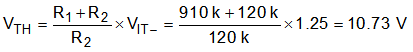
9.2.2 Detailed Design Procedure
To create two voltage monitoring rails, the PFI input can be used along with the MR pin to create a single output. The 5-V monitor is created by selecting a 5-V device option, giving threshold of 4.55 V. The PFI input is configured to any adjustable rail with a voltage divider. Use Equation 1 to select resistors.
Equation 1.