SBVS149B September 2010 – January 2016 TPS386000-Q1
PRODUCTION DATA.
- 1 Features
- 2 Applications
- 3 Description
- 4 Revision History
- 5 Pin Configuration and Functions
- 6 Specifications
- 7 Parametric Measurement information
- 8 Detailed Description
- 9 Application and Implementation
- 10Power Supply Recommendations
- 11Layout
- 12Device and Documentation Support
- 13Mechanical, Packaging, and Orderable Information
パッケージ・オプション
メカニカル・データ(パッケージ|ピン)
- RGP|20
サーマルパッド・メカニカル・データ
- RGP|20
発注情報
11 Layout
11.1 Layout Guidelines
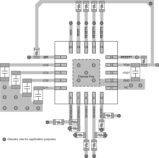
Follow these guidelines to lay out the printed-circuit-board (PCB) that is used for the TPS386000-Q1 family of devices.
- Keep the traces to the timer capacitors as short as possible to optimize accuracy.
- Avoid long traces from the SENSE pin to the resistor divider. Instead, run the long traces from the RSnH to VMON(n).
- Place the VDD decoupling capacitor (CVDD) close to the device.
- Avoid using long traces for the VDD supply node. The VDD capacitor (CVDD), along with parasitic inductance from the supply to the capacitor, can form an LC tank and create ringing with peak voltages above the maximum VDD voltage.
11.2 Layout Example
 Figure 35. Example Layout (RGP Package)