JAJSCZ8B March   2017  – February 2018 TPS3890-Q1

PRODUCTION DATA.  

  1. 特長
  2. アプリケーション
  3. 概要
    1.     Device Images
      1.      代表的なアプリケーション回路
      2.      VITNの精度と温度との関係
  4. 改訂履歴
  5. Device Comparison Table
  6. Pin Configuration and Functions
    1.     Pin Functions
  7. Specifications
    1. 7.1 Absolute Maximum Ratings
    2. 7.2 ESD Ratings
    3. 7.3 Recommended Operating Conditions
    4. 7.4 Thermal Information
    5. 7.5 Electrical Characteristics
    6. 7.6 Timing Requirements
    7. 7.7 Typical Characteristics
  8. Detailed Description
    1. 8.1 Overview
    2. 8.2 Functional Block Diagram
    3. 8.3 Feature Description
      1. 8.3.1 User-Configurable RESET Delay Time
      2. 8.3.2 Manual Reset (MR) Input
      3. 8.3.3 RESET Output
      4. 8.3.4 SENSE Input
        1. 8.3.4.1 Immunity to SENSE Pin Voltage Transients
    4. 8.4 Device Functional Modes
      1. 8.4.1 Normal Operation (VDD > VDD(min))
      2. 8.4.2 Above Power-On-Reset But Less Than VDD(min) (VPOR < VDD < VDD(min))
      3. 8.4.3 Below Power-On-Reset (VDD < VPOR)
  9. Application and Implementation
    1. 9.1 Application Information
    2. 9.2 Typical Application
      1. 9.2.1 Design Requirements
      2. 9.2.2 Detailed Design Procedure
      3. 9.2.3 Application Curve
  10. 10Power Supply Recommendations
  11. 11Layout
    1. 11.1 Layout Guidelines
    2. 11.2 Layout Example
  12. 12デバイスおよびドキュメントのサポート
    1. 12.1 デバイス・サポート
      1. 12.1.1 デバイスの項目表記
    2. 12.2 ドキュメントのサポート
      1. 12.2.1 関連資料
    3. 12.3 ドキュメントの更新通知を受け取る方法
    4. 12.4 コミュニティ・リソース
    5. 12.5 商標
    6. 12.6 静電気放電に関する注意事項
    7. 12.7 Glossary
  13. 13メカニカル、パッケージ、および注文情報

パッケージ・オプション

メカニカル・データ(パッケージ|ピン)
サーマルパッド・メカニカル・データ
発注情報

Typical Characteristics

over the operating junction temperature range of –40°C to +125°C, 1.5 V ≤ VDD ≤ 5.5 V, and MR = VDD (unless otherwise noted)
TPS3890-Q1 D001-SLVSD65-01_Vit-.gif
Figure 2. VITN Accuracy vs Temperature
TPS3890-Q1 D019_SLVSD65_Vitp_Histogrom.gif
Tested at VDD = 1.5 V and VDD = 5.5 V, total tests = 136,348
Figure 4. VITN Accuracy Histogram
TPS3890-Q1 D021_SLVSD65_Hyst_Histogrom.gif
Tested at VDD = 1.5 V and VDD = 5.5 V, total tests = 136,348
Figure 6. Hysteresis Histogram
TPS3890-Q1 D003-SLVSD65-01_Iq_MR_6p5V.gif
MR = VDD
Figure 8. Supply Current vs Power-Supply Voltage
TPS3890-Q1 D006-SLVSD65-03_MR_Thresh_VCC_1p5V.gif
VDD = 1.5 V
Figure 10. MR Threshold vs Temperature
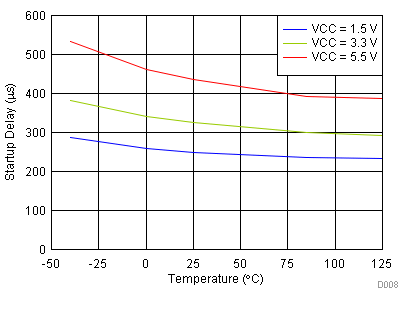
TPS3890-Q1 D008-SLVSD65-01_Startup_Delay.gif
Figure 12. Startup Delay vs Temperature
TPS3890-Q1 D010-SLVSD65-01_Prop_Delay_LH_1p5V.gif
VDD = 1.5 V
Figure 14. Propagation Delay (tPD(r)) vs Overdrive
TPS3890-Q1 D012-SLVSD65-01_Prop_Delay_HL_1p5V.gif
VDD = 1.5 V
Figure 16. Propagation Delay (tPD(f)) vs Overdrive
TPS3890-Q1 D014-SLVSD65-01_Glitch_Rejection_1p5V.gif
VDD = 1.5 V
Figure 18. Low-to-High Glitch Immunity vs Temperature
TPS3890-Q1 D018-SLVSD65-04.gif
VDD = 1.5 V
Figure 20. High-to-Low Glitch Immunity vs Temperature
TPS3890-Q1 D016-SLVSD65-01_Vol_1p5.gif
VDD = 1.5 V
Figure 22. Low-Level Output Voltage vs RESET Current
TPS3890-Q1 D002-SLVSD65-01_Vit_plus.gif
Figure 3. VITP Accuracy vs Temperature
TPS3890-Q1 D020_SLVSD65_Vitn_Histogrom.gif
Tested at VDD = 1.5 V and VDD = 5.5 V, total tests = 136,348
Figure 5. VITP Accuracy Histogram
TPS3890-Q1 D005-SLVSD65-01_CT_Current.gif
Figure 7. CT Current vs Temperature
TPS3890-Q1 D004-SLVSD65-02_Iq_MR_0V.gif
MR = 0 V
Figure 9. Supply Current vs Power-Supply Voltage
TPS3890-Q1 D007-SLVSD65-01_MR_Thresh_VCC_6p5V.gif
VDD = 5.5 V
Figure 11. MR Threshold vs Temperature
TPS3890-Q1 D009-SLVSD65-02_Prop_Delay_LH_6p5V.gif
VDD = 5.5 V
Figure 13. Propagation Delay (tPD(r)) vs Overdrive
TPS3890-Q1 D011-SLVSD65-02_Prop_Delay_HL_6p5V.gif
VDD = 5.5 V
Figure 15. Propagation Delay (tPD(f)) vs Overdrive
TPS3890-Q1 D013-SLVSD65-01_Glitch_Rejection_6p5V.gif
VDD = 5.5 V
Figure 17. Low-to-High Glitch Immunity vs Temperature
TPS3890-Q1 D017-SLVSD65-01.gif
VDD = 5.5 V
Figure 19. High-to-Low Glitch Immunity vs Temperature
TPS3890-Q1 D015-SLVSD65-02_Vol_5p5.gif
VDD = 5.5 V
Figure 21. Low-Level Output Voltage vs RESET Current