JAJSCZ8B March   2017  – February 2018 TPS3890-Q1

PRODUCTION DATA.  

  1. 特長
  2. アプリケーション
  3. 概要
    1.     Device Images
      1.      代表的なアプリケーション回路
      2.      VITNの精度と温度との関係
  4. 改訂履歴
  5. Device Comparison Table
  6. Pin Configuration and Functions
    1.     Pin Functions
  7. Specifications
    1. 7.1 Absolute Maximum Ratings
    2. 7.2 ESD Ratings
    3. 7.3 Recommended Operating Conditions
    4. 7.4 Thermal Information
    5. 7.5 Electrical Characteristics
    6. 7.6 Timing Requirements
    7. 7.7 Typical Characteristics
  8. Detailed Description
    1. 8.1 Overview
    2. 8.2 Functional Block Diagram
    3. 8.3 Feature Description
      1. 8.3.1 User-Configurable RESET Delay Time
      2. 8.3.2 Manual Reset (MR) Input
      3. 8.3.3 RESET Output
      4. 8.3.4 SENSE Input
        1. 8.3.4.1 Immunity to SENSE Pin Voltage Transients
    4. 8.4 Device Functional Modes
      1. 8.4.1 Normal Operation (VDD > VDD(min))
      2. 8.4.2 Above Power-On-Reset But Less Than VDD(min) (VPOR < VDD < VDD(min))
      3. 8.4.3 Below Power-On-Reset (VDD < VPOR)
  9. Application and Implementation
    1. 9.1 Application Information
    2. 9.2 Typical Application
      1. 9.2.1 Design Requirements
      2. 9.2.2 Detailed Design Procedure
      3. 9.2.3 Application Curve
  10. 10Power Supply Recommendations
  11. 11Layout
    1. 11.1 Layout Guidelines
    2. 11.2 Layout Example
  12. 12デバイスおよびドキュメントのサポート
    1. 12.1 デバイス・サポート
      1. 12.1.1 デバイスの項目表記
    2. 12.2 ドキュメントのサポート
      1. 12.2.1 関連資料
    3. 12.3 ドキュメントの更新通知を受け取る方法
    4. 12.4 コミュニティ・リソース
    5. 12.5 商標
    6. 12.6 静電気放電に関する注意事項
    7. 12.7 Glossary
  13. 13メカニカル、パッケージ、および注文情報

パッケージ・オプション

メカニカル・データ(パッケージ|ピン)
サーマルパッド・メカニカル・データ
発注情報

Manual Reset (MR) Input

The manual reset (MR) input allows a processor or other logic circuits to initiate a reset. A logic low on MR causes RESET to assert. After MR returns to a logic high and SENSE is above VITP, RESET is deasserted after the user-defined reset delay. If MR is not controlled externally, then MR must be connected to VDD. Note that if the logic signal driving MR is not greater than or equal to VDD, then some additional current flows into VDD and out of MR and the difference is apparent when comparing Figure 8 and Figure 9.

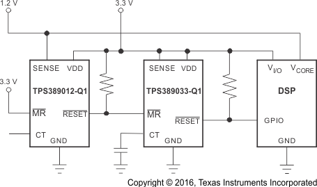
Figure 23 shows how MR can be used to monitor multiple system voltages when only a single CT capacitor is needed to set the RESET delay time.
TPS3890-Q1 fbd_mr_monitor_volts_sbvs303.gifFigure 23. Using MR to Monitor Multiple System Voltages