SLUSAF8E July 2011 – January 2016 TPS40322
PRODUCTION DATA.
- 1 Features
- 2 Applications
- 3 Description
- 4 Revision History
- 5 Pin Configuration and Functions
- 6 Specifications
-
7 Detailed Description
- 7.1 Overview
- 7.2 Functional Block Diagram
- 7.3
Feature Description
- 7.3.1 Voltage Reference
- 7.3.2 Output Voltage Setting
- 7.3.3 Input Voltage Feedforward
- 7.3.4 Current Sensing
- 7.3.5 Overcurrent Protection
- 7.3.6 Two-Phase Mode, Remote Sense Amplifier, and Current Sharing Loop
- 7.3.7 Start-Up and Shutdown
- 7.3.8 Switching Frequency and Master or Slave Synchronization
- 7.3.9 Overvoltage and Undervoltage Fault Protection
- 7.3.10 Input Undervoltage Lockout (UVLO)
- 7.3.11 Power Good
- 7.3.12 Thermal Shutdown
- 7.3.13 Connection of Unused Pins
- 7.4 Device Functional Modes
-
8 Applications and Implementation
- 8.1 Application Information
- 8.2
Typical Applications
- 8.2.1
Dual-Output Configuration from 12-V Nominal to 1.2-V and 1.8-V DC-to-DC Converter Using the TPS40322
- 8.2.1.1 Design Requirements
- 8.2.1.2
Detailed Design Procedure
- 8.2.1.2.1 Selecting a Switching Frequency
- 8.2.1.2.2 Inductor Selection (L1)
- 8.2.1.2.3 Output Capacitor Selection (C10 through C16)
- 8.2.1.2.4 Peak Current Rating of Inductor
- 8.2.1.2.5 Input Capacitor Selection (C3 through C6)
- 8.2.1.2.6 MOSFET Selection (Q1)
- 8.2.1.2.7 ILIM Resistor (R2)
- 8.2.1.2.8 Feedback Divider (R10, R14)
- 8.2.1.2.9 Compensation: (R11, R12, C17, C19, C21)
- 8.2.1.2.10 Boot-Strap Capacitor (C7)
- 8.2.1.2.11
General Device Components
- 8.2.1.2.11.1 Synchronization (SYNC Pin)
- 8.2.1.2.11.2 RT Resistor (R6)
- 8.2.1.2.11.3 Differential Amplifier Out (DIFFO Pin)
- 8.2.1.2.11.4 EN/SS Timing Capacitors (C8)
- 8.2.1.2.11.5 Power Good (PG1, PG2 Pins)
- 8.2.1.2.11.6 Phase Set (PHSET Pin)
- 8.2.1.2.11.7 UVLO Programming Resistors (R1 and R3)
- 8.2.1.2.11.8 VDD Bypass Capacitor (C2)
- 8.2.1.2.11.9 VBP6 Bypass Capacitor (C18)
- 8.2.1.3 Application Curves
- 8.2.2 Two-Phase, Single Output Configuration from 12-V nominal to 1.2-V DC-to-DC Converter Using the TPS40322
- 8.2.1
Dual-Output Configuration from 12-V Nominal to 1.2-V and 1.8-V DC-to-DC Converter Using the TPS40322
- 9 Power Supply Recommendations
- 10Layout
- 11Device and Documentation Support
- 12Mechanical, Packaging, and Orderable Information
パッケージ・オプション
メカニカル・データ(パッケージ|ピン)
- RHB|32
サーマルパッド・メカニカル・データ
- RHB|32
発注情報
8 Applications and Implementation
NOTE
Information in the following applications sections is not part of the TI component specification, and TI does not warrant its accuracy or completeness. TI’s customers are responsible for determining suitability of components for their purposes. Customers should validate and test their design implementation to confirm system functionality.
8.1 Application Information
The TPS40322 is a dual-output, synchronous buck controller, and it can also be configured as a two-phase controller.
8.2 Typical Applications
8.2.1 Dual-Output Configuration from 12-V Nominal to 1.2-V and 1.8-V DC-to-DC Converter Using the TPS40322
This section explains the design process and component selection for a dual output synchronous buck converter using TPS40322 controller. The design goal parameters are listed in Table 3. The design procedure provides calculations for channel 1 only. User can apply similar calculation for channel 2.
Figure 23 shows the dual output converter schematic for this design example.
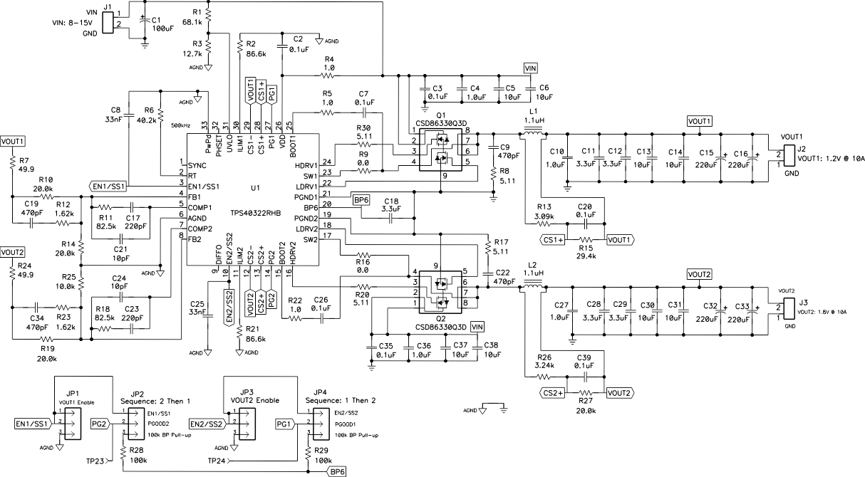 Figure 23. Design Example 1, Dual Output Converter Schematic
8.2.1.1 Design Requirements
The design goal parameters are listed in Table 3.
Table 3. TPS40322 Dual Output Design Example Specification
| PARAMETER | TEST CONDITION | MIN | TYP | MAX | UNIT | |
|---|---|---|---|---|---|---|
| INPUT CHARACTERISTICS | ||||||
| VIN | Input voltage | 8 | 12 | 15 | V | |
| VIN(ripple) | Input ripple | IOUT1 = IOUT2 = 10 A | 0.25 | V | ||
| OUTPUT 1 CHARACTERISTICS | ||||||
| VOUT1 | Output voltage | IOUT1(min) ≤ IOUT1 ≤ IOUT1(max) | 1.2 | V | ||
| Line regulation | VIN(min) ≤ VIN ≤ VIN(max) | 0.5% | ||||
| Load regulation | IOUT1(min) ≤ IOUT1 ≤ IOUT1(max) | 0.5% | ||||
| VRIPPLE1 | Output ripple | IOUT1 = IOUT1(max) | 24 | mV | ||
| VOVER1 | Output overshoot | ΔIOUT1 = 5 A | 40 | mV | ||
| VUNDER1 | Output undershoot | ΔIOUT1 = 5A | 40 | mV | ||
| IOUT1 | Output current | VIN(min) ≤ VIN ≤ VIN(max) | 0 | 10 | A | |
| ISCP1 | Short circuit current trip point | 15 | A | |||
| OUTPUT 2 CHARACTERISTICS | ||||||
| VOUT2 | Output voltage | IOUT2(min) ≤ IOUT2 ≤ IOUT2(max) | 1.8 | V | ||
| Line regulation | VIN(min) ≤ VIN ≤ VIN(max) | 0.5% | ||||
| Load regulation | IOUT2(min) ≤ IOUT2 ≤ IOUT2(max) | 0.5% | ||||
| VRIPPLE2 | Output ripple | IOUT2 = IOUT2(max) | 36 | mV | ||
| VOVER2 | Output overshoot | ΔIOUT2 = 5 A | 40 | mV | ||
| VUNDER2 | Output undershoot | ΔIOUT2 = 5 A | 40 | mV | ||
| IOUT2 | Output current | VIN(min) ≤ VIN ≤ VIN(max) | 0 | 10 | A | |
| ISCP2 | Short circuit current trip point | 15 | A | |||
| GENERAL CHARACTERSTICS | ||||||
| tSS | Soft-start time | VIN = 12 V | 2 | ms | ||
| η | Efficiency | VIN = 12 V, IOUT1= IOUT2 = 10 A | 88% | |||
| fSW | Switching frequency | 500 | kHz | |||
8.2.1.2 Detailed Design Procedure
Inductor Selection (L1) through General Device Components show equations and calculations regarding VOUT1. VOUT2 values can be calculated using similar equations. See Table 4 for the list of materials.
Table 4. Design Example 1, Dual-Output List of Materials
| REFERENCE DESIGNATOR |
QTY | DESCRIPTION | PART NUMBER | MFR |
|---|---|---|---|---|
| C1 | 1 | Capacitor, Aluminum, 100 µF, 35 V, ±20%, 0.328 x 0.328 inch | EEV-FK1V101GP | Panasonic - ECG |
| C2, C7, C20, C26, C39 | 5 | Capacitor, Ceramic, 0.1 µF, 50 V, X7R, ±10%, 0603 | Std | Std |
| C3, C35 | 2 | Capacitor, Ceramic, 0.1 µF, 25 V, X5R, ±10%, 0402 | Std | Std |
| C4, C36 | 2 | Capacitor, Ceramic, 1.0 µF, 25 V, X7R, ±10%, 0603 | Std | Std |
| C5, C6, C37, C38 | 4 | Capacitor, Ceramic, 10 µF, 25 V, X5R, ±10%, 0805 | Std | Std |
| C8, C25 | 2 | Capacitor, Ceramic, 33 nF, 16 V, X7R, ±10%, 0603 | Std | Std |
| C9, C19, C22, C34 | 4 | Capacitor, Ceramic, 470 pF, 25 V, C0G, NP0, ±5%, 0603 | Std | Std |
| C10, C27 | 2 | Capacitor, Ceramic, 1.0 µF, 6.3 V, X5R, ±10%, 0402 | Std | Std |
| C11, C12, C18, C28, C29 | 5 | Capacitor, Ceramic, 3.3 µF, 10 V, X5R, ±10%, 0603 | C1608X5R1A335K | TDK Corporation |
| C13, C14, C30, C31 | 4 | Capacitor, Ceramic, 10 µF, 6.3 V, X7R, ±10%, 0805 | Std | Std |
| C15, C16, C32, C33 | 4 | Capacitor, Polymer Aluminum, 220 µF, 4 V, ±20%, 5 mΩ ESR | EEF-SE0G221ER | Panasonic - ECG |
| C17, C23 | 2 | Capacitor, Ceramic, 220 pF, 50 V, C0G, NP0, ±5%, 0603 | Std | Std |
| C21, C24 | 2 | Capacitor, Ceramic, 10 pF, 50 V, C0G, NP0, ±5%, 0603 | Std | Std |
| C40 | 1 | Capacitor, Ceramic, 1.0 nF, 25 V, C0G, NP0, ±5%, 0603 | Std | Std |
| L1, L2 | 2 | Inductor, Power Choke, 1.1 µH, ±20%, 3.15 mΩ, 7.0 mm x 6.9 mm | 744314110 | Wurth Elektronik |
| Q1, Q2 | 2 | MOSFET, Synchronous Buck NexFET Power Block, QFN-8 POWER | CSD86330Q3D | Texas Instruments |
| R1 | 1 | Resistor, Chip, 68.1 kΩ, 1/10 W, ±1%, 0603 | Std | Std |
| R2, R21 | 2 | Resistor, Chip, 86.6 kΩ, 1/10 W, ±1%, 0603 | Std | Std |
| R3 | 1 | Resistor, Chip, 12.7 kΩ, 1/10 W, ±1%, 0603 | Std | Std |
| R4, R5, R22 | 3 | Resistor, Chip, 1.00 Ω, 1/10 W, ±1%, 0603 | Std | Std |
| R6 | 1 | Resistor, Chip, 40.2 kΩ, 1/10 W, ±1%, 0603 | Std | Std |
| R7, R24 | 2 | Resistor, Chip, 49.9 Ω, 1/10 W, ±1%, 0603 | Std | Std |
| R8, R17 | 2 | Resistor, Chip, 5.11 Ω, 1/8 W, ±1%, 0805 | Std | Std |
| R9, R16 | 2 | Resistor, Chip, 0 Ω, 1/10 W, ±1%, 0603 | Std | Std |
| R10, R14, R19, R27 | 4 | Resistor, Chip, 20.0 kΩ, 1/10 W, ±1%, 0603 | Std | Std |
| R11, R18 | 2 | Resistor, Chip, 82.5 kΩ, 1/10 W, ±1%, 0603 | Std | Std |
| R12, R23 | 2 | Resistor, Chip, 1.62 kΩ, 1/10 W, ±1%, 0603 | Std | Std |
| R13 | 1 | Resistor, Chip, 3.09 kΩ, 1/10 W, ±1%, 0603 | Std | Std |
| R15 | 1 | Resistor, Chip, 29.4 kΩ, 1/10 W, ±1%, 0603 | Std | Std |
| R20, R30 | 2 | Resistor, Chip, 5.11 Ω, 1/10 W, ±1%, 0603 | Std | Std |
| R25 | 1 | Resistor, Chip, 10.0 kΩ, 1/10 W, ±1%, 0603 | Std | Std |
| R26 | 1 | Resistor, Chip, 3.24 kΩ, 1/10 W, ±1%, 0603 | Std | Std |
| R28, R29 | 2 | Resistor, Chip, 100 kΩ, 1/10 W, ±1%, 0603 | Std | Std |
| U1 | 1 | TPS40322 Dual Synchronous Buck Controller, QFN-32 | TPS40322RHB | Texas Instruments |
8.2.1.2.1 Selecting a Switching Frequency
To maintain acceptable efficiency and meet minimum on-time requirements, a 500-kHz switching frequency is selected.
8.2.1.2.2 Inductor Selection (L1)
Synchronous BUCK power inductors are typically sized for approximately 20%–40% peak-to-peak ripple current (IRIPPLE). Given a target ripple current of 30%, the required inductor size, at maximum rated output current, can be calculated using Equation 8.

Selecting a standard, readily available inductor, with a rated inductance is 0.88 µH at 10 A, IRIPPLE1 = 2.5 A.
The RMS current through the inductor is approximated by the equation:

8.2.1.2.3 Output Capacitor Selection (C10 through C16)
The selection of the output capacitor is typically driven by the output transient response requirement. Equation 10 and Equation 11 over-estimate the voltage deviation to account for delays in the loop bandwidth and can be used to determine the required output capacitance:


When VIN(min) > 2 x VOUT1, use the overshoot equation, VOVER1, to calculate minimum output capacitance. When VIN(min) < 2 x VOUT1 use Equation 11, VUNDER1, to calculate minimum output capacitance. In this design example, VIN(min) is much larger than 2 x VOUT1 so Equation 12 is used to determine the required minimum output capacitance.

With a minimum capacitance, the maximum allowable ESR is determined by the maximum ripple voltage and is approximated by Equation 13.

Two 220-µF, 4-V, aluminum electrolytic capacitors were chosen for load response requirements. Additionally two 0805 10-µF, X7R, along with two 0603, 3.3-µF X5R, and one 1-µF, X5R ceramic capacitors are selected for low ESR and high frequency decoupling.
8.2.1.2.4 Peak Current Rating of Inductor
With the output capacitance known, it is possible to calculate the charge current during start-up and determine the minimum saturation current rating for the inductor. The start-up charging current is approximated using Equation 14.


Table 5. Inductor Requirements Summary
| PARAMETER | VALUE | UNIT | |
|---|---|---|---|
| L1 | Inductance | 0.88 | µH |
| IL1_RMS | RMS current (thermal rating) | 10.026 | A |
| IL1_PEAK | Peak current (saturation rating) | 11.53 | A |
A 744314110 from Wurth Electronics with 1.1-µH zero current inductance is selected. Inductance for this part is 0.88-µH at 10-A bias. This 15-A, 3.15-mΩ inductor exceeds the minimum inductor ratings in a 7-mm x 7-mm package.
8.2.1.2.5 Input Capacitor Selection (C3 through C6)
The input voltage ripple is divided between the capacitance and ESR of the input capacitor. For this design VRIPPLE(cap) = 200 mV and VRIPPLE(esr) = 50 mV. The minimum capacitance and maximum ESR are estimated using Equation 16.


The RMS current in the input capacitors is estimated using Equation 18.


To achieve these goals, two 0805, 10-µF capacitors, one 0605, 1.0-µF capacitor and one 0402, 0.1-µF X5R ceramic capacitor are combined at the input.
8.2.1.2.6 MOSFET Selection (Q1)
Texas Instruments CSD86330, 20-A power block device was chosen. This device incorporates the high-side and low-side MOSFETs in a single 3 mm x 3 mm package. The high-side MOSFET has an on-resistance (RDS(on)) of 8.8 mΩ, while the low-side on-resistance (RDS(on)) is 4.6 mΩ, both at 4.5 V gate voltage. A 5.11-Ω gate resistor is used on the HDRV pin on each device for added noise immunity.
8.2.1.2.7 ILIM Resistor (R2)
The output current is sensed across the DCR of the L1 output inductor. An RC combination having a time constant equal to that of the L1 inductance and the DCR is used to extract the current information as a voltage. A standard capacitor value of 0.1-µF is used. The resistor, R13, can be calculated using Equation 20.

A standard 3.09-kΩ resistor was selected.
This design limits the maximum voltage drop across the current sense inputs, VCS(max), to 50 mV. If the voltage drop across the DCR of the inductor is greater than VCS(max), after allowing for 20% overshoot spikes and a 20% variation in the DCR value, then a resistor is added to divide the voltage down to 50 mV. The divider resistor, R15, is calculated by Equation 21.

where
- VDCR = (DCR × 1.2) × (IL(peak) × 1.2)
The maximum DCR voltage drop is given by Equation 22.

The current limit resistor is calculated using the minimum ILIM programming current, IILIM(min), the maximum current sense amplifier gain, ACS, and assuming a current sense amplifier minimum input offset voltage, VOS(min) equal to –3 mV.
8.2.1.2.8 Feedback Divider (R10, R14)
The TPS40322 controller uses a full operational amplifier with an internally fixed 0.600-V reference. Tha value for R10 is selected between 10-kΩ and 50-kΩ for a balance of feedback current and noise immunity. With the R10 resistor set to 20-kΩ, the output voltage is programmed with a resistor divider given by Equation 24.

8.2.1.2.9 Compensation: (R11, R12, C17, C19, C21)
Using the TPS40k Loop Stability Tool for an 85-kHz bandwidth and 50° of phase margin with an R10 value of 20.0 kΩ, and measuring the theoretical results in the laboratory and modifying accordingly for system optimization yields the following values:
- C21 = 10 pF
- C17 = 220 pF
- C19 = 470 pF
- R12 = 4.42 kΩ
- R11 = 82.5 kΩ
8.2.1.2.10 Boot-Strap Capacitor (C7)
To ensure proper charging of the high-side FET gate, limit the ripple voltage on the boost capacitor to < 100 mV.

8.2.1.2.11 General Device Components
8.2.1.2.11.1 Synchronization (SYNC Pin)
The SYNC pin must be left open for independent dual outputs.
8.2.1.2.11.2 RT Resistor (R6)
The desired switching frequency is programmed by the current through RRT to GND. the value of RRT is calculated using Equation 26.

8.2.1.2.11.3 Differential Amplifier Out (DIFFO Pin)
In dual output configuration the DIFFO pin is not used and must remain open (unconnected).
8.2.1.2.11.4 EN/SS Timing Capacitors (C8)
The soft-start capacitor provides smooth ramp of the error amplifier reference voltage for controlled start-up. The soft-start capacitor is selected using Equation 27.

8.2.1.2.11.5 Power Good (PG1, PG2 Pins)
PG1 and PG2 can each be pulled up to BP6 through a 100-kΩ resistor, or remain not-connected. For sequencing the start-up of output 1 before output 2, connect PG1 to EN2/SS2; for sequencing the start-up of output 2 before output 1, connect PG2 to EN1/SS1.
8.2.1.2.11.6 Phase Set (PHSET Pin)
The PHSET pin can be connected to ground or connected to the BP6 pin.
8.2.1.2.11.7 UVLO Programming Resistors (R1 and R3)
The UVLO hysteresis level is programmed by R1 with Equation 28 and Equation 29.


8.2.1.2.11.8 VDD Bypass Capacitor (C2)
As shown in the Pin Configuration and Functions section, use a 0.1-µF, 50-V, X7R capacitor for VDD bypass.
8.2.1.2.11.9 VBP6 Bypass Capacitor (C18)
Select a 3.3-µF (or greater) low ESR capacitor for BP6. For this design use a 3.3-µF, X5R ceramic capacitor.
8.2.1.3 Application Curves
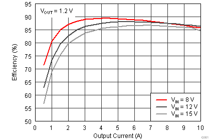 Figure 24. Efficiency vs Load Current (8 V to 15 V to 1.2 V at 10 A, Design Example 1)
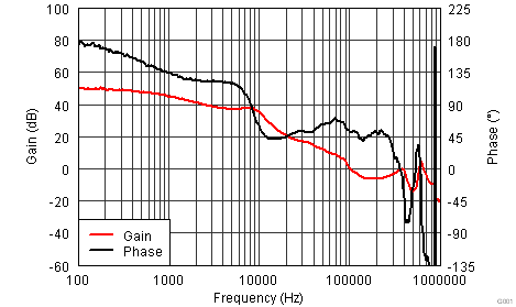 Figure 26. Design Example 1 Loop Response
VIN = 12 V, VOUT1 = 1.2 V, IOUT1 = 10 A, 80-kHz Bandwidth, 50° Phase Margin
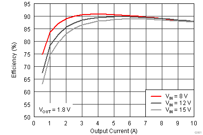 Figure 25. Efficiency vs Load Current (8 V to 15 V to 1.8 V at 10 A, Design Example 1)
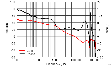 Figure 27. Design Example 1 Loop Response
VIN = 12 V, VOUT2 = 1.8 V, IOUT2 = 10 A, 80-kHz Bandwidth, 50° Phase Margin
Figure 28 shows the switching waveform, VIN = 12 V, IOUT1 = IOUT2 = 10 A, Ch.1 = HDRV1, Ch.2 = LDRV1, Ch.3 = VOUT1 ripple. The high-frequency noise is caused by parasitic inductive and capacitive elements interacting with the high energy, rapidly switching power elements resulting in ringing at the transition points. Capacitive filtering at the load input will successfully attenuate these noise spikes.
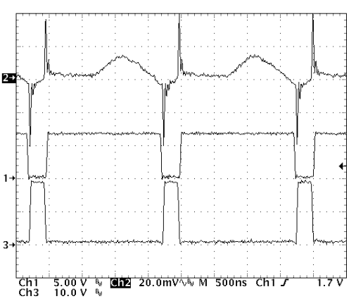 Figure 28. Design Example 1 Switching Waveform
8.2.2 Two-Phase, Single Output Configuration from 12-V nominal to 1.2-V DC-to-DC Converter Using the TPS40322
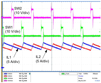
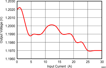
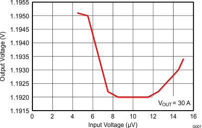
Figure 29 shows the schematic, waveforms, and components for a two-phase, single output synchronous buck converter using the TPS40322 controller. The design goal parameters are given in Table 7.
Table 6 summaries the channel 2 related pin connection in two-phase mode.
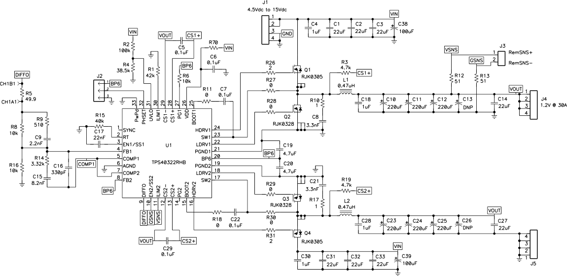 Figure 29. Design Example 2, Two-Phase Converter Schematic
Table 6. Channel 2 Pin Connections in Two-Phase Mode
| PIN NAME | CONNECTION | |||
|---|---|---|---|---|
| COMP2 | Connect to COMP1 | |||
| EN2/SS2/GSNS | Use as GSNS pin, connect to the output ground | |||
| FB2 | Connect to BP6 | |||
| ILIM2/VSNS | Use as VSNS pin, connect to output | |||
| PG2 | Floating or connect to ground | |||
8.2.2.1 Design Requirements
The design goal parameters are listed in Table 7.
Table 7. TPS40322 Design Example 2 Specification
| PARAMETER | TEST CONDITION | MIN | TYP | MAX | UNIT | |
|---|---|---|---|---|---|---|
| VIN | Input voltage | 4.5 | 15 | V | ||
| VOUT | Output voltage | IOUT(min) ≤ IOUT ≤ IOUT(max) | 1.2 | V | ||
| Line regulation | VIN(min) ≤ VIN ≤ VIN(max) | 0.5% | ||||
| Load regulation | IOUT(min) ≤ IOUT ≤ IOUT(max) | 0.5% | ||||
| VRIPPLE | Output ripple | IOUT1 = IOUT1(max) | 12 | mV | ||
| VOVER | Output overshoot | ΔIOUT1 = 5 A | 40 | mV | ||
| VUNDER | Output undershoot | ΔIOUT1 = 5A | 40 | mV | ||
| IOUT | Output current | VIN(min) ≤ VIN ≤ VIN(max) | 0 | 30 | A | |
| tSS | Soft-start time | VIN = 12 V | 2 | ms | ||
| η | Efficiency | VIN = 12 V, IOUT1 = IOUT2 = 10 A | 88% | |||
| fSW | Switching frequency | 500 | kHz | |||
8.2.2.2 Detailed Design Procedure
Inductor Selection (L1) through General Device Components show equations and calculations regarding VOUT1. VOUT2 values can be calculated using similar equations. See Table 8 for the list of materials.
Table 8. TPS40322 Design Example 2, Two-Phase, Single Output Bill of Materials
| REFERENCE DESIGNATOR |
QTY | DESCRIPTION | PART NUMBER | MFR |
|---|---|---|---|---|
| C1, C2, C3, C31, C32, C33 | 6 | Capacitor, Ceramic, 22 µF, 25 V, X5R, ±20%, 1210 | Std | Std |
| C4, C18, C28, C30 | 4 | Capacitor, Ceramic, 1 µF, 50 V, X7R, ±10%, 0603 | Std | Std |
| C5, C6, C7, C22, C29 | 5 | Capacitor, Ceramic, 0.1 µF, 50 V, X7R, ±10%, 0603 | Std | Std |
| C8, C21 | 2 | Capacitor, Ceramic, 6.8 nF, 50 V, X7R, ±10%, 0805 | Std | Std |
| C9 | 1 | Capacitor, Ceramic, 2.2 nF, 16 V, X7R, ±10%, 0603 | Std | Std |
| C10, C11, C12, C13, C23, C24, C25, C26 | 8 | Capacitor, Polymer Aluminum, 220 µF, 4 V, ±20%, 5mΩ ESR | EEFSE0G221R | Panasonic - ECG |
| C14, C27 | 2 | Capacitor, Ceramic, 22 µF, 6.3 V, X5R, ±10%, 0805 | Std | Std |
| C15 | 1 | Capacitor, Ceramic, 8.2 nF, 16 V, X7R, ±10%, 0603 | Std | Std |
| C16 | 1 | Capacitor, Ceramic, 330 pF, 16 V, X7R, ±10%, 0603 | Std | Std |
| C17 | 1 | Capacitor, Ceramic, 22 nF, 50 V, X7R, ±10%, 0603 | Std | Std |
| C19, C20 | 2 | Capacitor, Ceramic, 4.7 µF, 16 V, X7R, ±10%, 0805 | Std | Std |
| C38, C39 | 2 | Capacitor, Aluminum, 100 µF, 25 V, ±20%, F8 | ECE-V1EA101XP | Panasonic - ECG |
| L1, L2 | 2 | Inductor, SMT, 0.47 µH, ±20%, 1.2 mΩ, 0.512" x 0.571" | IHLP5050FDERR47M01 | Vishay/Dale |
| Q1, Q4 | 2 | MOSFET, N-channel, 30 V, 30 A, 8 mΩ, 5-LFPAK | RJK0305 | Renesas Electronics |
| Q2, Q3 | 2 | MOSFET, N-channel, 30 V, 60 A, 2.1 mΩ, 5-LFPAK | RJK0328 | Renesas Electronics |
| R1 | 1 | Resistor, Chip, 42 kΩ, 1/10 W, ±1%, 0603 | Std | Std |
| R2 | 1 | Resistor, Chip, 100 kΩ, 1/10 W, ±1%, 0603 | Std | Std |
| R3, R19 | 2 | Resistor, Chip, 4.7 kΩ, 1/10 W, ±1%, 0603 | Std | Std |
| R4 | 1 | Resistor, Chip, 38.5 kΩ, 1/10 W, ±1%, 0603 | Std | Std |
| R5 | 1 | Resistor, Chip, 49.9 Ω, 1/10 W, ±1%, 0603 | Std | Std |
| R6, R8, R16 | 3 | Resistor, Chip, 10 kΩ, 1/10 W, ±1%, 0603 | Std | Std |
| R7, R27, R28, R29, R30 | 5 | Resistor, Chip, 0 Ω, 1/10 W, ±1%, 0603 | Std | Std |
| R9 | 1 | Resistor, Chip, 511 Ω, 1/10 W, ±1% | Std | Std |
| R10, R17 | 1 | Resistor, Chip, 1.00 Ω, 1/8 W, ±1%, 0805 | Std | Std |
| R11, R18 | 2 | Resistor, Chip, 5.11 Ω, 1/10 W, ±1% 0603 | 603 | Std |
| R12, R13 | 2 | Resistor, Chip, 51 Ω, 1/10 W, ±1%, 0603 | Std | Std |
| R14 | 1 | Resistor, Chip, 3.32 kΩ, 1/10 W, ±1%, 0603 | Std | Std |
| R15 | 1 | Resistor, Chip, 40 kΩ, 1/10 W, ±1%, 0603 | Std | Std |
| R26, R31 | 2 | Resistor, Chip, 2 Ω, 1/10 W, ±1%, 0603 | Std | Std |
| R20, R21, R22, R23, R24, R25, | 0 | not used | Std | Std |
| U1 | 1 | Dual synchronous buck controller, QFN-32 | TPS40322RHB | Texas Instruments |
8.2.2.3 Application Curves
