SLVS616C November 2005 – December 2014 TPS51124
PRODUCTION DATA.
- 1 Features
- 2 Applications
- 3 Description
- 4 Revision History
- 5 Pin Configuration and Functions
- 6 Specifications
- 7 Detailed Description
- 8 Application and Implementation
- 9 Power Supply Recommendations
- 10Layout
- 11Device and Documentation Support
- 12Mechanical, Packaging, and Orderable Information
10 Layout
10.1 Layout Guidelines
Certain points must be considered before starting a layout using the TPS51124.
- Connect RC low-pass filter from V5IN to V5FILT, 1-μF and 3.3-Ω are recommended. Place the filter capacitor close to the IC, within 12 mm (0.5 inch) if possible.
- Connect the over-current setting resistors from TRIPx to GND, and as close as possible to the IC. The trace from TRIPx to resistor, and resistor to GND, should avoid coupling to high-voltage switching node.
- The discharge path (VOx) should have a dedicated trace to the output capacitor(s), separate from the output voltage sensing trace. Use 1,5-mm (60 mils) or wider trace, with no loops. Tie the feedback-current-setting resistor (the resistor between VFBx to GND) close to the IC’s GND. The trace from this resistor to VFBx pin should be short and thin. Place on the component side and avoid vias between this resistor and the IC.
- Connections from the drivers to the respective gate of the high-side or the low-side MOSFET should be as short as possible to reduce stray inductance. Use 0,65-mm (25 mils) or wider trace.
- All sensitive analog traces and components such as VOx, VFBx, GND, ENx, PGOODx, TRIPx, V5FILT, and TONSEL should be placed away from high-voltage switching nodes such as LLx, DRVLx, DRVHx, or VBSTx nodes to avoid coupling. Use internal layer(s) as ground plane(s) and shield the feedback trace from power traces and components.
- Gather ground terminal of VIN capacitor(s), Vout capacitor(s), and source of low-side MOSFETs as close as possible. GND (signal ground) and PGNDx (power ground) should be connected strongly together near the IC. PCB trace defined as LLx node, which connects to source of high-side MOSFET, drain of low-side MOSFET and high-voltage side of the inductor, should be as short and wide as possible.
- In order to effectively remove heat from the package, prepare thermal land and solder to the package’s thermal pad. Two by two or more vias with a 0,33-mm (13 mils) diameter connected from the thermal land to the internal ground plane should be used to help dissipation. Do NOT connect PGNDx to this thermal land underneath the package.
10.2 Layout Example
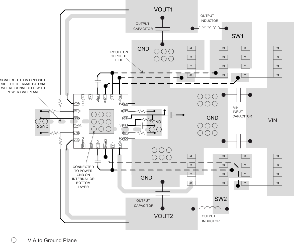 Figure 26. Layout Example