JAJSC08E MAY   2011  – July 2018 TPS51206

PRODUCTION DATA.  

  1. 特長
  2. アプリケーション
  3. 概要
    1.     Device Images
      1.      単純化したアプリケーションの図
  4. 改訂履歴
  5. Pin Configuration and Functions
    1.     Pin Functions
  6. Specifications
    1. 6.1 Absolute Maximum Ratings
    2. 6.2 ESD Ratings
    3. 6.3 Recommended Operating Conditions
    4. 6.4 Thermal Information
    5. 6.5 Electrical Characteristics
    6. 6.6 Typical Characteristics
  7. Detailed Description
    1. 7.1 Overview
    2. 7.2 Functional Block Diagram
    3. 7.3 Feature Description
      1. 7.3.1 VTT Sink and Source Regulator
      2. 7.3.2 VTTREF
      3. 7.3.3 VDD Undervoltage Lockout Protection
      4. 7.3.4 VTT Current Limit
      5. 7.3.5 Overtemperature Protection
      6. 7.3.6 Power On and Off Sequence
    4. 7.4 Device Functional Modes
      1. 7.4.1 Power State Control
  8. Application and Implementation
    1. 8.1 Application Information
    2. 8.2 Typical Applications
      1. 8.2.1 VLDOIN = VDDQ Configuration
        1. 8.2.1.1 Design Requirements
        2. 8.2.1.2 Detailed Design Procedure
          1. 8.2.1.2.1 VDD Capacitor
          2. 8.2.1.2.2 VLDOIN Capacitor
          3. 8.2.1.2.3 VTTREF Capacitor
          4. 8.2.1.2.4 VTT Capacitor
          5. 8.2.1.2.5 VTTSNS Connection
          6. 8.2.1.2.6 VDDQSNS Connection
        3. 8.2.1.3 Application Curves
      2. 8.2.2 VLDOIN Separated from VDDQ Configuration
        1. 8.2.2.1 Design Requirements
        2. 8.2.2.2 Detailed Design Procedure
        3. 8.2.2.3 Application Curves
  9. Power Supply Recommendations
  10. 10Layout
    1. 10.1 Layout Guidelines
    2. 10.2 Layout Example
    3. 10.3 Thermal Considerations
  11. 11デバイスおよびドキュメントのサポート
    1. 11.1 デバイス・サポート
      1. 11.1.1 デベロッパー・ネットワークの製品に関する免責事項
    2. 11.2 ドキュメントの更新通知を受け取る方法
    3. 11.3 コミュニティ・リソース
    4. 11.4 商標
    5. 11.5 静電気放電に関する注意事項
    6. 11.6 Glossary
  12. 12メカニカル、パッケージ、および注文情報

パッケージ・オプション

メカニカル・データ(パッケージ|ピン)
サーマルパッド・メカニカル・データ
発注情報

Power On and Off Sequence

Figure 23 is the recommended power on and off sequence. During power on, it is allowed to turn on VDD, S3 and S5 first, then turn on VLDOIN and VDDQSNS. During power off, it is allowed to turn off VDD, S3 and S5 first, then turn off VLDOIN and VDDQSNS.
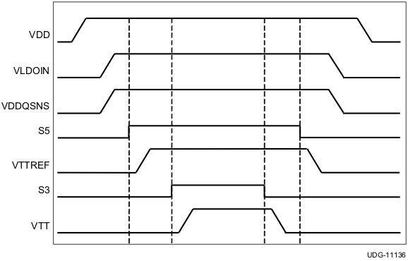
TPS51206 v11036_lusah1.gifFigure 23. Typical Timing Diagram