SLVSBM7A March 2013 – January 2016 TPS54061-Q1
PRODUCTION DATA.
- 1 Features
- 2 Applications
- 3 Description
- 4 Revision History
- 5 Pin Configuration and Functions
- 6 Specifications
-
7 Detailed Description
- 7.1 Overview
- 7.2 Functional Block Diagram
- 7.3
Feature Description
- 7.3.1 Fixed Frequency PWM Control
- 7.3.2 Slope Compensation Output Current
- 7.3.3 Error Amplifier
- 7.3.4 Voltage Reference
- 7.3.5 Adjusting the Output Voltage
- 7.3.6 Enable and Adjusting Undervoltage Lockout (UVLO)
- 7.3.7 Internal Slow-Start
- 7.3.8 Constant Switching Frequency and Timing Resistor (RT/CLK Pin)
- 7.3.9 Selecting the Switching Frequency
- 7.3.10 Synchronization to RT/CLK Pin
- 7.3.11 Overvoltage Protection
- 7.3.12 Thermal Shutdown
- 7.4 Device Functional Modes
-
8 Applications and Implementation
- 8.1 Application Information
- 8.2
Typical Applications
- 8.2.1
Continuous Conduction Mode Application
- 8.2.1.1 Design Requirements
- 8.2.1.2
Detailed Design Procedure
- 8.2.1.2.1 Selecting the Switching Frequency
- 8.2.1.2.2 Output Inductor Selection (LO)
- 8.2.1.2.3 Output Capacitor
- 8.2.1.2.4 Input Capacitor
- 8.2.1.2.5 Bootstrap Capacitor Selection
- 8.2.1.2.6 Undervoltage Lockout Set Point
- 8.2.1.2.7 Output Voltage and Feedback Resistors Selection
- 8.2.1.2.8 Closing the Loop
- 8.2.1.3 Application Curves
- 8.2.2 Discontinuous Conduction Mode Application
- 8.2.1
Continuous Conduction Mode Application
- 9 Power Supply Recommendations
- 10Layout
- 11Device and Documentation Support
- 12Mechanical, Packaging, and Orderable Information
パッケージ・オプション
メカニカル・データ(パッケージ|ピン)
- DRB|8
サーマルパッド・メカニカル・データ
- DRB|8
発注情報
6 Specifications
6.1 Absolute Maximum Ratings
over operating free-air temperature range (unless otherwise noted)(1)| MIN | MAX | UNIT | ||
|---|---|---|---|---|
| Voltage | VIN | –0.3 | 62 | V |
| EN(2) | –0.3 | 8 | V | |
| BOOT-PH | 8 | V | ||
| BOOT | 70 | V | ||
| VSENSE | –0.3 | 6 | V | |
| COMP | –0.3 | 3 | V | |
| PH | –0.6 | 62 | V | |
| PH, 10-ns transient | –2 | 62 | V | |
| RT/CLK | –0.3 | 6 | V | |
| Current | VIN | Internally limited | A | |
| BOOT | 100 | mA | ||
| PH | Internally limited | A | ||
| Operating junction temperature | –40 | 150 | ºC | |
| Storage temperature, Tstg | –65 | 150 | ºC | |
(1) Stresses beyond those listed under Absolute Maximum Ratings may cause permanent damage to the device. These are stress ratings only, which do not imply functional operation of the device at these or any other conditions beyond those indicated under Recommended Operating Conditions. Exposure to absolute-maximum-rated conditions for extended periods may affect device reliability.
6.2 ESD Ratings
| VALUE | UNIT | |||
|---|---|---|---|---|
| V(ESD) | Electrostatic discharge | Human body model (HBM), per QSS 009-105 (JESD22-A114A) and AEC-Q100 Classification Level H2(1) | ±2000 | V |
| Charged-device model (CDM), per QSS 009-147 (JESD22-C101B.01) and AEC-Q100 500V Classification Level C3B(2) | ±750 | |||
(1) JEDEC document JEP155 states that 500-V HBM allows safe manufacturing with a standard ESD control process.
(2) JEDEC document JEP157 states that 250-V CDM allows safe manufacturing with a standard ESD control process.
6.3 Recommended Operating Conditions
over operating free-air temperature range (unless otherwise noted)| MIN | MAX | UNIT | ||
|---|---|---|---|---|
| Input voltage, VIN | 4.7 | 60 | V | |
| Output current | 200 | mA | ||
| Switching frequency set by RT/CLK resistor | 50 | 1100 | kHz | |
| Switching frequency synchronized to external clock | 300 | 1100 | kHz | |
6.4 Thermal Information
| THERMAL METRIC(1) | TPS54061-Q1 | UNIT | ||
|---|---|---|---|---|
| DRB (SON) | ||||
| 8 PINS | ||||
| RθJA | Junction-to-ambient thermal resistance | 42.9 | °C/W | |
| RθJC(top) | Junction-to-case (top) thermal resistance | 46.0 | °C/W | |
| RθJB | Junction-to-board thermal resistance | 18.1 | °C/W | |
| ψJT | Junction-to-top characterization parameter | 0.5 | °C/W | |
| ψJB | Junction-to-board characterization parameter | 18.3 | °C/W | |
| RθJC(bot) | Junction-to-case (bottom) thermal resistance | 3.0 | °C/W | |
(1) For more information about traditional and new thermal metrics, see the Semiconductor and IC Package Thermal Metrics application report, SPRA953.
6.5 Electrical Characteristics
TJ = –40°C to 150°C, VIN = 4.7 to 60 V (unless otherwise noted)(1)| PARAMETER | CONDITIONS | MIN | TYP | MAX | UNIT |
|---|---|---|---|---|---|
| SUPPLY VOLTAGE (VIN PIN) | |||||
| Operating input voltage | 4.7 | 60 | V | ||
| Shutdown supply current | EN = 0 V | 1.4 | µA | ||
| IQ operating; non-switching | VSENSE = 0.9 V, VIN = 12 V | 90 | 110 | µA | |
| ENABLE AND UVLO (EN PIN) | |||||
| Enable threshold | Rising | 1.23 | 1.4 | V | |
| Falling | 1 | 1.18 | V | ||
| Input current | Enable threshold 50 mV | –4.7 | µA | ||
| Enable threshold –50 mV | –1.2 | µA | |||
| Hysteresis | –3.5 | µA | |||
| Enable high to start switching time | 450 | µs | |||
| VIN | |||||
| VIN start voltage | VIN rising | 4.5 | V | ||
| VOLTAGE REFERENCE | |||||
| Voltage reference | TJ = 25°C, VIN = 12 V | 0.792 | 0.8 | 0.808 | V |
| 1 mA < IOUT < Minimum current limit | 0.784 | 0.8 | 0.816 | ||
| HIGH-SIDE MOSFET | |||||
| Switch resistance | BOOT-PH = 5.7 V | 1.5 | 3 | Ω | |
| LOW-SIDE MOSFET | |||||
| Switch resistance | VIN = 12 V | 0.8 | 1.5 | Ω | |
| ERROR AMPLIFIER | |||||
| Input current | VSENSE pin | 20 | nA | ||
| Error-amplifier gm | –2 µA < I(COMP) < 2 µA, V(COMP) = 1 V | 108 | µMhos | ||
| EA gm during slow-start | –2 µA < I(COMP) < 2 µA, V(COMP) = 1 V, VSENSE = 0.4 V | 27 | µMhos | ||
| Error amplifier DC gain | VSENSE = 0.8 V | 1000 | V/V | ||
| Minimum unity-gain bandwidth | 0.5 | MHz | |||
| Error amplifier source and sink | V(COMP) = 1 V, 100-mV overdrive | ±8 | µA | ||
| Start-switching threshold | 0.57 | V | |||
| COMP to Iswitch gm | 1 | A/V | |||
| CURRENT LIMIT | |||||
| High-side sourcing current-limit threshold | BOOT-PH = 5.7 V | 250 | 350 | 500 | mA |
| Zero-cross detect current | –1.1 | mA | |||
| THERMAL SHUTDOWN | |||||
| Thermal shutdown | 176 | C | |||
| RT/CLK | |||||
| Operating frequency using RT mode | 50 | 1100 | kHz | ||
| Switching frequency | R(RT/CLK) = 120 kΩ | 425 | 472 | 520 | kHz |
| Minimum CLK pulse duration | 40 | ns | |||
| RT/CLK voltage | R(RT/CLK) = 120 kΩ | 0.53 | V | ||
| RT/CLK high threshold | 1.8 | V | |||
| RT/CLK low threshold | 0.5 | V | |||
| RT/CLK falling-edge to PH rising-edge delay | Measure at 500 kHz with RT resistor | 67 | ns | ||
| PLL lock-in time | Measure at 500 kHz | 100 | µs | ||
| PLL frequency range | 300 | 1100 | kHz | ||
| PH | |||||
| Minimum ON-time | Measured at 50% to 50%, IOUT = 200 mA | 120 | ns | ||
| Dead time | VIN = 12 V, IOUT = 200 mA, one transition | 30 | ns | ||
| BOOT | |||||
| BOOT-to-PH regulation voltage | VIN = 12 V | 6 | V | ||
| BOOT-PH UVLO | 2.9 | V | |||
| INTERNAL SLOW-START TIME | |||||
| Slow-start time | fSW = 472 kHz, RT = 120 kΩ, 10% to 90% | 2.36 | ms | ||
(1) The electrical ratings specified in this section apply to all specifications in this document unless otherwise noted. These specifications are interpreted as conditions that do not degrade the parametric or functional specifications of the device for the life of the product containing it.
6.6 Typical Characteristics
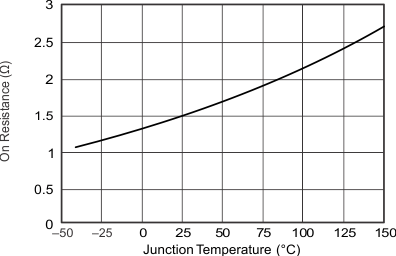
| VIN = 12 V |
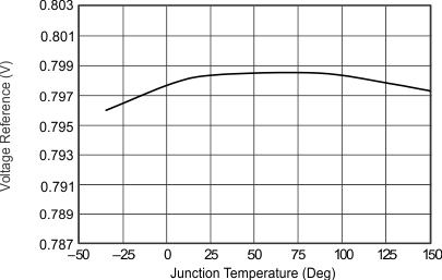
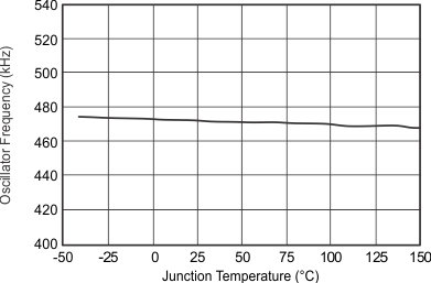
| VIN = 12 V | RT = 120 kΩ |
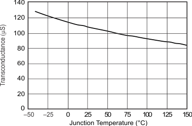
| VIN = 12 V |
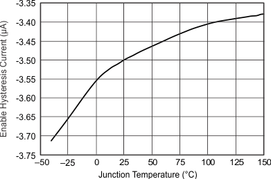
| VIN = 12 V |
vs Temperature
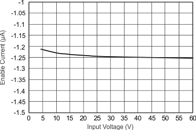
| VIN = 12 V | TJ = 25°C |
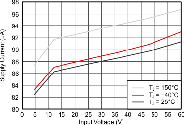
| EN = Open | VSENSE = 0.83 V |
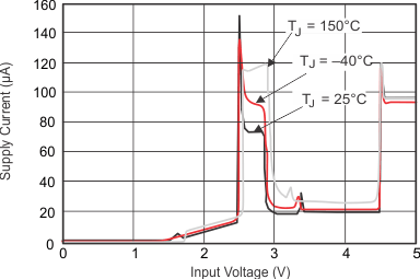
| EN = Open |
Input Voltage (0 V to VSTART), EN Pin Open
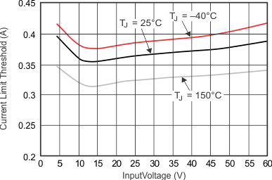
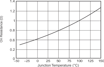
| VIN = 12 V |
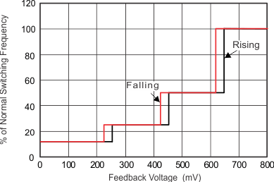
| VIN = 12 V | RT = 120 kΩ | TJ = 25°C |
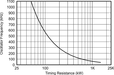
| VIN = 12 V | TJ = 25°C |
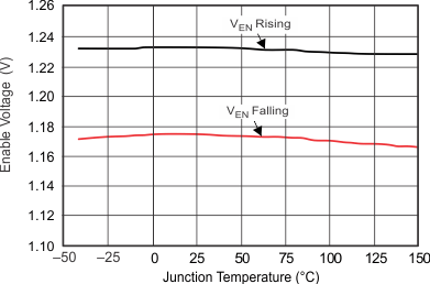
| VIN = 12 V |
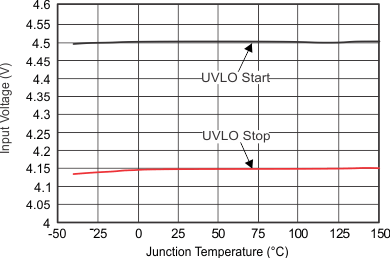
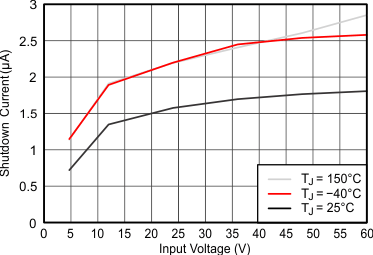
| EN = 0 V |
vs Input Voltage
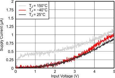
| EN = 0 V |
vs Input Voltage (0 V to VSTART), EN Pin Low
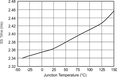
| VIN = 12 V | fsw = 472 kHz |