JAJSD91A June 2017 – April 2021 TPS54308
PRODUCTION DATA
- 1 特長
- 2 アプリケーション
- 3 概要
- 4 Revision History
- 5 Pin Configuration and Functions
- 6 Specifications
-
7 Detailed Description
- 7.1 Overview
- 7.2 Functional Block Diagram
- 7.3
Feature Description
- 7.3.1 Fixed-Frequency PWM Control
- 7.3.2 Force Continuous Conduction Mode (FCCM)
- 7.3.3 Error Amplifier
- 7.3.4 Slope Compensation and Output Current
- 7.3.5 Enable and Adjusting Undervoltage Lockout
- 7.3.6 Safe Start-Up into Pre-Biased Outputs
- 7.3.7 Voltage Reference
- 7.3.8 Adjusting Output Voltage
- 7.3.9 Internal Soft Start
- 7.3.10 Bootstrap Voltage (BOOT)
- 7.3.11 Overcurrent Protection
- 7.3.12 Output Overvoltage Protection (OVP)
- 7.3.13 Thermal Shutdown
- 7.4 Device Functional Modes
-
8 Application and Implementation
- 8.1 Application Information
- 8.2
Typical Application
- 8.2.1 TPS54308 8-V to 28-V Input, 5-V Output Converter
- 8.2.2 Design Requirements
- 8.2.3 Detailed Design Procedure
- 8.2.4 Application Curves
- 9 Power Supply Recommendations
- 10Layout
- 11Device and Documentation Support
- 12Mechanical, Packaging, and Orderable Information
8.2.3.6.3 Feedforward Capacitor
The TPS54308 is internally compensated. The internal compensation network is composed of two capacitors and one resister shown on the block diagram. Depending on the VOUT, if the output capacitor COUT is dominated by low ESR (ceramic types) capacitors, it can result in low phase margin. To improve the phase boost, an external feedforward capacitor C6 can be added in parallel with R2. C6 is chosen such that phase margin is boosted at the crossover frequency.
Equation 16 for C6 was tested:
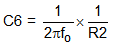
For this design, feedforward capacitor C6 is not needed since load transient performance looks good and meets design requirement. If further boosting phase margin for low-ESR (ceramic types) capacitors is desired, useTable 8-2 as a starting point for the feedforward capacitor choosing. It also recommends in series with one 2-kΩ resistor (R6) with this feedforward capacitor to get better steady-state performance under high VIN with a heavy load.
| VOUT (V) | L (µH) | COUT (µF) | R2 (kΩ) | R3 (kΩ) | C6 (µF) | R6 (kΩ) |
|---|---|---|---|---|---|---|
| 1.8 | 5.6 | 66 | 100 | 49.9 | 47 | 2 |
| 2.5 | 6.8 | 66 | 100 | 31.6 | 47 | 2 |
| 3.3 | 10 | 44 | 100 | 22.1 | 75 | 2 |
| 5 | 15 | 44 | 100 | 13.3 | 75 | 2 |
| 12 | 22 | 44 | 100 | 5.23 | 100 | 2 |