SLVS932F May 2009 – November 2014 TPS54325
PRODUCTION DATA.
- 1 Features
- 2 Applications
- 3 Description
- 4 Simplified Schematic
- 5 Revision History
- 6 Pin Configuration and Functions
- 7 Specifications
- 8 Detailed Description
- 9 Application and Implementation
- 10Power Supply Recommendations
- 11Layout
- 12Device and Documentation Support
- 13Mechanical, Packaging, and Orderable Information
8 Detailed Description
8.1 Overview
The TPS54325 is a 3-A synchronous step-down (buck) converter with two integrated N-channel MOSFETs. It operates using D-CAP2™ mode control. The fast transient response of D-CAP2™ control reduces the output capacitance required to meet a specific level of performance. Proprietary internal circuitry allows the use of low ESR output capacitors including ceramic and special polymer types.
8.2 Functional Block Diagram
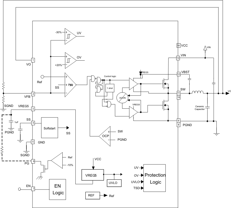
8.3 Feature Description
8.3.1 Soft Start and Pre-Biased Soft Start
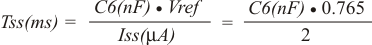
The TPS54325 has an adjustable soft start . When the EN pin becomes high, 2.0-μA current begins charging the capacitor which is connected from the SS pin to GND. Smooth control of the output voltage is maintained during start up. The equation for the slow start time is shown in Equation 1. VFB voltage is 0.765 V and SS pin source current is 2 μA.
The TPS54325 contains a unique circuit to prevent current from being pulled from the output during startup in the condition the output is pre-biased. When the soft-start commands a voltage higher than the pre-bias level (internal soft start becomes greater than feedback voltage (VFB), the controller slowly activates synchronous rectification by starting the first low side FET gate driver pulses with a narrow on-time. It then increments that on-time on a cycle-by-cycle basis until it coincides with the time dictated by (1-D), where D is the duty cycle of the converter. This scheme prevents the initial sinking of the pre-bias output, and ensure that the out voltage (VO) starts and ramps up smoothly into regulation and the control loop is given time to transition from pre-biased start-up to normal mode operation.
8.3.2 Power Good
The TPS54325 has power-good output. The power-good function is activated after soft start has finished. If the output voltage becomes within -10% of the target value, internal comparators detect power good state and the power good signal becomes high. RPG resister value ,which is connected between PG and VREG5, is required from 20 kΩ to 150 kΩ. If the feedback voltage goes under 15% of the target value, the power good signal becomes low after 10 μs internal delay.
8.3.3 Output Discharge Control
The TPS54325 discharges the output when EN is low, or the controller is turned off by the protection functions (OVP, UVP, UVLO and thermal shutdown). The device discharges outputs using an internal 50-Ω MOSFET which is connected to VO and PGND. The internal low-side MOSFET is not turned on during the output discharge operation to avoid the possibility of causing negative voltage at the output.
8.3.4 Current Protection
The output over-current protection (OCP) is implemented using a cycle-by-cycle valley detect control circuit. The switch current is monitored by measuring the low-side FET switch voltage between the SW pin and GND. This voltage is proportional to the switch current. To improve accuracy, the voltage sensing is temperature compensated.
During the on time of the high-side FET switch, the switch current increases at a linear rate determined by VIN, VOUT, the on-time and the output inductor value. During the on time of the low-side FET switch, this current decreases linearly. The average value of the switch current is the load current Iout. If the measured voltage is above the voltage proportional to the current limit, Then , the device constantly monitors the low-side FET switch voltage, which is proportional to the switch current, during the low-side on-time.
The converter maintains the low-side switch on until the measured voltage is below the voltage corresponding to the current limit at which time the switching cycle is terminated and a new switching cycle begins. In subsequent switching cycles, the on-time is set to a fixed value and the current is monitored in the same manner.
There are some important considerations for this type of over-current protection. The load current one half of the peak-to-peak inductor current higher than the over-current threshold. Also when the current is being limited, the output voltage tends to fall as the demanded load current may be higher than the current available from the converter. This may cause the output under-voltage protection circuit to be activated. When the over current condition is removed, the output voltage will return to the regulated value. This protection is non-latching.
8.3.5 Overvoltage and Undervoltage Protection
The TPS54325 monitors a resistor divided feedback voltage to detect over and under voltage. When the feedback voltage becomes higher than 120% of the target voltage, the OVP comparator output goes high and the circuit latches the high-side MOSFET driver turns off and the low-side MOSFET turns on.
When the feedback voltage becomes lower than 70% of the target voltage, the UVP comparator output goes high and an internal UVP delay counter begins. After 250 μs, the device latches off both internal top and bottom MOSFET. This function is enabled approximately 1.7 x soft-start time.
8.3.6 UVLO Protection
The TPS54325 has under voltage lock out protection (UVLO) that monitors the voltage of VREG5 pin. When the VREG5 voltage is lower than UVLO threshold voltage, the TPS54325 is shut off. This is non-latch protection.
8.3.7 Thermal Shutdown
The TPS54325 monitors the temperature of itself. If the temperature exceeds the threshold value (typically 150°C), the device is shut off. This is non-latch protection.
8.4 Device Functional Modes
8.4.1 PWM Operation
The main control loop of the TPS54325 is an adaptive on-time pulse width modulation (PWM) controller that supports a proprietary D-CAP2™ mode control. D-CAP2™ mode control combines constant on-time control with an internal compensation circuit for pseudo-fixed frequency and low external component count configuration with both low ESR and ceramic output capacitors. It is stable even with virtually no ripple at the output.
At the beginning of each cycle, the high-side MOSFET is turned on. This MOSFET is turned off after internal one shot timer expires. This one shot timer is set by the converter input voltage ,VIN, and the output voltage ,VO, to maintain a pseudo-fixed frequency over the input voltage range, hence it is called adaptive on-time control. The one-shot timer is reset and the high-side MOSFET is turned on again when the feedback voltage falls below the reference voltage. An internal ramp is added to the reference voltage to simulate output ripple, eliminating the need for ESR induced output ripple from D-CAP2™ mode control.
8.4.2 PWM Frequency and Adaptive On-Time Control
TPS54325 uses an adaptive on-time control scheme and does not have a dedicated on board oscillator. The TPS54325 runs with a pseudo-constant frequency of 700 kHz by using the input voltage and output voltage to set the on-time one-shot timer. The on-time is inversely proportional to the input voltage and proportional to the output voltage, therefore, when the duty ratio is VOUT/VIN, the frequency is constant.
8.4.3 Operation with VIN < 4.5 V
The device is recommended to operate with input voltages above 4.5 V. The typical VIN UVLO threshold is 3.7 V and the device can operate at input voltages down to the UVLO voltage. At input voltages below the actual UVLO voltage, the device does not switch. If the EN pin is externally pulled up or left floating, the device becomes active when the VIN pin passes the UVLO threshold. Switching begins when the slow-start sequence is initiated.
8.4.4 Operation With EN Control
The enable threshold voltage is 1.6 V (typical). With the EN pin is held below that voltage, the device is disabled and switching is inhibited even if the VIN pin is above the UVLO threshold. The IC quiescent current is reduced in this state. If the EN voltage increases above the threshold while the VIN pin is above the UVLO threshold, the device becomes active. Switching is then enabled and the slow-start sequence is initiated.