JAJSIZ2B october 2016 – june 2021 TPS54388C-Q1
PRODUCTION DATA
- 1 特長
- 2 アプリケーション
- 3 概要
- 4 Revision History
- 5 Pin Configuration and Functions
- 6 Specifications
-
7 Detailed Description
- 7.1 Overview
- 7.2 Functional Block Diagram
- 7.3 Feature Description
- 7.4
Device Functional Modes
- 7.4.1 Adjusting the Output Voltage
- 7.4.2 Enable Functionality and Adjusting Undervoltage Lockout
- 7.4.3 Slow-Start or Tracking Pin
- 7.4.4 Sequencing
- 7.4.5 Constant Switching Frequency and Timing Resistor (RT/CLK Pin)
- 7.4.6 Overcurrent Protection
- 7.4.7 Frequency Shift
- 7.4.8 Reverse Overcurrent Protection
- 7.4.9 Synchronize Using the RT/CLK Pin
- 7.4.10 Power Good (PWRGD Pin)
- 7.4.11 Overvoltage Transient Protection
- 7.4.12 Thermal Shutdown
- 7.4.13 Small-Signal Model for Loop Response
- 7.4.14 Simple Small-Signal Model for Peak-Current-Mode Control
- 7.4.15 Small-Signal Model for Frequency Compensation
-
8 Application and Implementation
- 8.1 Application Information
- 8.2
Typical Application
- 8.2.1 Design Requirements
- 8.2.2
Detailed Design Procedure
- 8.2.2.1 Selecting the Switching Frequency
- 8.2.2.2 Output Inductor Selection
- 8.2.2.3 Output Capacitor
- 8.2.2.4 Input Capacitor
- 8.2.2.5 Slow-Start Capacitor
- 8.2.2.6 Bootstrap Capacitor Selection
- 8.2.2.7 Output-Voltage and Feedback-Resistor Selection
- 8.2.2.8 Compensation
- 8.2.2.9 Power-Dissipation Estimate
- 8.2.3 Application Curves
- 9 Power Supply Recommendations
- 10Layout
- 11Device and Documentation Support
- 12Mechanical, Packaging, and Orderable Information
パッケージ・オプション
メカニカル・データ(パッケージ|ピン)
- RTE|16
サーマルパッド・メカニカル・データ
- RTE|16
発注情報
7.4.5 Constant Switching Frequency and Timing Resistor (RT/CLK Pin)
The switching frequency of the TPS54388C-Q1 device is adjustable over a wide range from 200 kHz to 2000 kHz by placing a resistor on the RT/CLK pin with a value calculated by Equation 8. An internal amplifier holds this pin at a fixed voltage when using an external resistor to ground to set the switching frequency. The voltage on RT/CLK is typically 0.5 V. To determine the timing resistance for a given switching frequency, use Equation 8 or the curve in Figure 6-5.
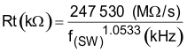
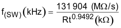
To reduce the solution size, one would typically set the switching frequency as high as possible, but consider tradeoffs of the efficiency, maximum input voltage, and minimum controllable on-time.
The minimum controllable on-time is typically 60 ns at full-current load and 120 ns at no load, and limits the maximum operating input voltage or output voltage.