JAJSDM2 July 2017 TPS54424
PRODUCTION DATA.
- 1 特長
- 2 アプリケーション
- 3 概要
- 4 改訂履歴
- 5 Pin Configuration and Functions
- 6 Specifications
-
7 Detailed Description
- 7.1 Overview
- 7.2 Functional Block Diagram
- 7.3
Feature Description
- 7.3.1 Fixed Frequency PWM Control
- 7.3.2 Continuous Conduction Mode Operation (CCM)
- 7.3.3 VIN Pins and VIN UVLO
- 7.3.4 Voltage Reference and Adjusting the Output Voltage
- 7.3.5 Error Amplifier
- 7.3.6 Enable and Adjustable UVLO
- 7.3.7 Soft Start and Tracking
- 7.3.8 Safe Start-up into Pre-Biased Outputs
- 7.3.9 Power Good
- 7.3.10 Sequencing (SS/TRK)
- 7.3.11 Adjustable Switching Frequency (RT Mode)
- 7.3.12 Synchronization (CLK Mode)
- 7.3.13 Bootstrap Voltage and 100% Duty Cycle Operation (BOOT)
- 7.3.14 Output Overvoltage Protection (OVP)
- 7.3.15 Overcurrent Protection
- 7.4 Device Functional Modes
-
8 Application and Implementation
- 8.1 Application Information
- 8.2
Typical Application
- 8.2.1 Design Requirements
- 8.2.2
Detailed Design Procedure
- 8.2.2.1 Custom Design With WEBENCH® Tools
- 8.2.2.2 Switching Frequency
- 8.2.2.3 Output Inductor Selection
- 8.2.2.4 Output Capacitor
- 8.2.2.5 Input Capacitor
- 8.2.2.6 Output Voltage Resistors Selection
- 8.2.2.7 Soft-start Capacitor Selection
- 8.2.2.8 Undervoltage Lockout Set Point
- 8.2.2.9 Bootstrap Capacitor Selection
- 8.2.2.10 PGOOD Pull-up Resistor
- 8.2.2.11 Compensation
- 8.2.3 Application Curves
- 9 Power Supply Recommendations
- 10Layout
- 11デバイスおよびドキュメントのサポート
- 12メカニカル、パッケージ、および注文情報
7 Detailed Description
7.1 Overview
The TPS54424 is a 17-V, 4-A, synchronous step-down (buck) converter with two integrated n-channel MOSFETs. To improve performance during line and load transients the device implements a constant frequency, peak current mode control which also simplifies external frequency compensation. The wide switching frequency of 200 kHz to 1600 kHz allows for efficiency and size optimization when selecting the output filter components. The switching frequency is adjusted using a resistor to ground on the RT/CLK pin. The TPS54424 also has an internal phase lock loop (PLL) connected to the RT/CLK pin that can be used to synchronize the switching cycle to the falling edge of an external system clock.
The integrated MOSFETs allow for high efficiency power supply designs with continuous output currents up to 4 amperes. The MOSFETs have been sized to optimize efficiency for lower duty cycle applications. The device reduces the external component count by integrating a bootstrap recharge circuit. The bias voltage for the integrated high-side MOSFET is supplied by a capacitor between the BOOT and SW pins. The BOOT capacitor voltage is monitored by a BOOT to SW UVLO (BOOT-SW UVLO) circuit allowing SW pin to be pulled low to recharge the BOOT capacitor. The device can operate at 100% duty cycle as long as the BOOT capacitor voltage is higher than the preset BOOT-SW UVLO threshold which is typically 2.2 V.
The TPS54424 has been designed for safe monotonic startup into pre-biased loads. The default start up is when VIN is typically 4.1 V. The EN pin has an internal pull-up current source that can be used to adjust the input voltage under voltage lockout (UVLO) with two external resistors. In addition, the internal pull-up current of the EN pin allows the device to operate with the EN pin floating. The operating current for the TPS54424 is typically 580 μA when not switching and under no load. When the device is disabled, the supply current is typically 3 μA.
The SS/TRK (soft start/tracking) pin is used to minimize inrush currents or provide power supply sequencing during power up. A small value capacitor or resistor divider should be coupled to the pin for soft start or critical power supply sequencing requirements. The output voltage can be stepped down to as low as the 0.6 V voltage reference (VREF). The device has a power good comparator (PGOOD) with hysteresis which monitors the output voltage through the FB pin. The PGOOD pin is an open drain MOSFET which is pulled low when the FB pin voltage is less than 89% or greater than 108% of the reference voltage VREF and asserts high when the FB pin voltage is 91% to 106% of VREF.
The device is protected from output overvoltage, overload and thermal fault conditions. The device minimizes excessive output overvoltage transients by taking advantage of the overvoltage circuit power good comparator. When the overvoltage comparator is activated, the high-side MOSFET is turned off and prevented from turning on until the FB pin voltage is lower than 106% of the VREF. The device implements both high-side MOSFET over current protection and bidirectional low-side MOSFET over current protections which help control the inductor current and avoid current runaway. The device also shuts down if the junction temperature is higher than thermal shutdown trip point. The device is restarted under control of the soft start circuit automatically when the junction temperature drops 15°C typically below the thermal shutdown trip point.
7.2 Functional Block Diagram
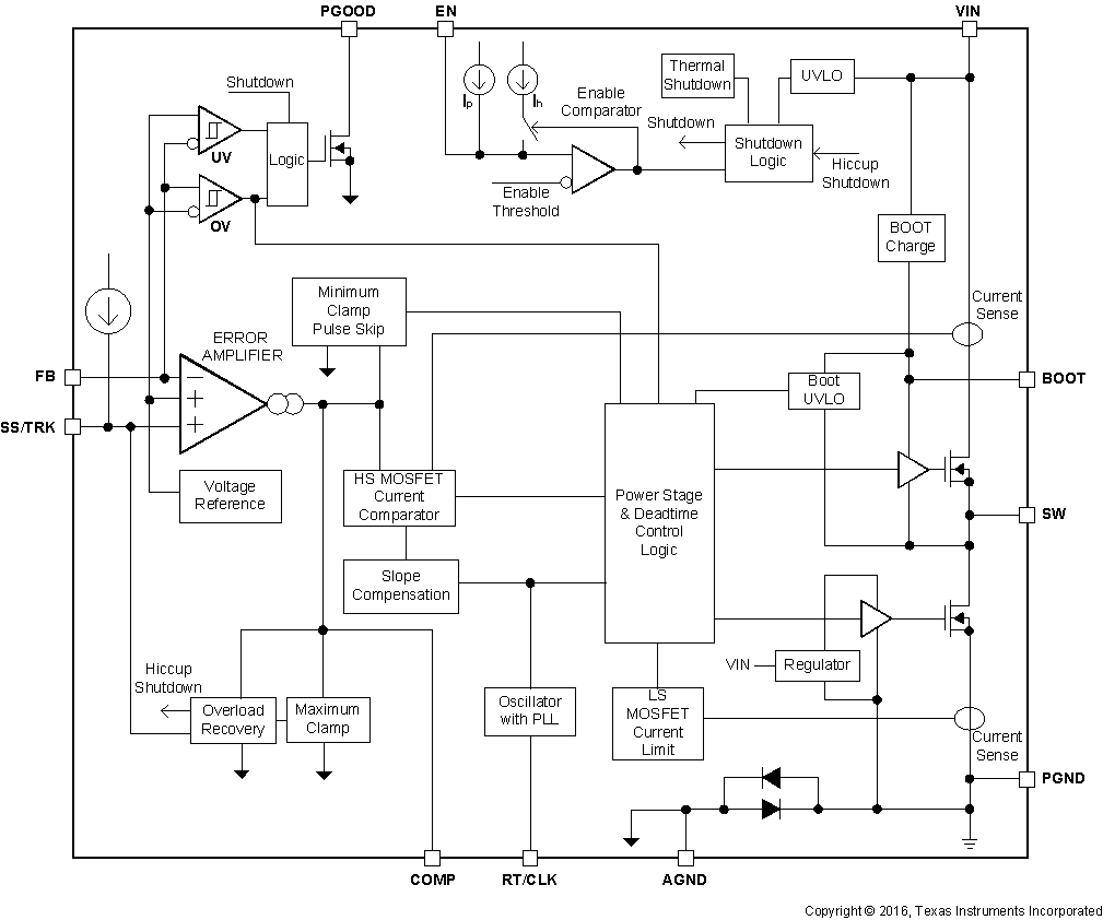
7.3 Feature Description
7.3.1 Fixed Frequency PWM Control
The device uses an adjustable fixed frequency, peak current mode control. The output voltage is compared through external resistors on the FB pin to an internal voltage reference by an error amplifier which drives the COMP pin. An internal oscillator initiates the turn on of the high-side power switch. The error amplifier output is converted into a current reference which compares to the high-side power switch current. When the power switch current reaches current reference generated by the COMP voltage level the high-side power switch is turned off and the low-side power switch is turned on.
The device adds an internal slope compensation ramp to prevent subharmonic oscillations. The peak inductor current limit remains constant over the full duty cycle range.
7.3.2 Continuous Conduction Mode Operation (CCM)
As a synchronous buck converter, the device works in CCM (Continuous Conduction Mode) under all load conditions.
7.3.3 VIN Pins and VIN UVLO
The VIN pin voltage supplies the internal control circuits of the device and provides the input voltage to the power converter system. The input voltage for VIN can range from 4.5 V to 17 V. The device implements internal UVLO circuitry on the VIN pin. The device is disabled when the VIN pin voltage falls below the internal VIN UVLO threshold. The internal VIN UVLO threshold has a hysteresis of 200 mV. A voltage divider connected to the EN pin can adjust the input voltage UVLO appropriately. See Enable and Adjustable UVLO for more details.
7.3.4 Voltage Reference and Adjusting the Output Voltage
The voltage reference system produces a precise ±0.85%, 0.6 V voltage reference over temperature by scaling the output of a temperature stable band gap circuit. The output voltage is set with a resistor divider from the output (VOUT) to the FB pin shown in Figure 26. It is recommended to use 1% tolerance or better divider resistors. Start with a fixed value for the bottom resistor in the divider, typically 10 kΩ, then use Equation 1 to calculate the top resistor in the divider. To improve efficiency at light loads consider using larger value resistors. If the values are too high the regulator is more susceptible to noise and voltage errors from the FB input current are noticeable. The minimum output voltage and maximum output voltage can be limited by the minimum on time of the high side MOSFET and bootstrap voltage (BOOT-SW voltage) respectively.
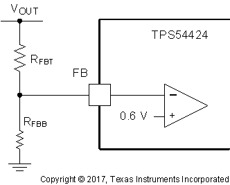 Figure 26. FB Resistor Divider

7.3.5 Error Amplifier
The device uses a transconductance error amplifier. The error amplifier compares the FB pin voltage to the lower of the SS/TRK pin voltage or the internal 0.6-V voltage reference. The transconductance of the error amplifier is 1100 μA/V. The frequency compensation network is connected between the COMP pin and ground.
When operating at current limit the COMP pin voltage is clamped to a maximum level to improve response when the load current decreases. When FB is greater than the internal voltage reference or SS/TRK the COMP pin voltage is clamped to a minimum level and the devices enters a high-side skip mode.
7.3.6 Enable and Adjustable UVLO
The EN pin provides on/off control of the device. Once the EN pin voltage exceeds its threshold voltage, the device starts operation. If the EN pin voltage is pulled below the threshold voltage, the regulator stops switching and enters low operating current state. The EN pin has an internal pull-up current source, Ip, allowing the user to float the EN pin for enabling the device. If an application requires controlling the EN pin, an open drain or open collector output logic can be interfaced with the pin.
An external resistor divider can be added from VIN to the EN pin for adjustable UVLO and hysteresis as shown in Figure 27. The EN pin has a small pull-up current Ip which sets the default state of the pin to enable when no external components are connected. The pull-up current is also used to control the voltage hysteresis for the UVLO function since it increases by Ih once the EN pin crosses the enable threshold. The UVLO thresholds can be calculated using Equation 2 and Equation 3. When using the adjustable UVLO function, 500 mV or greater hysteresis is recommended. For applications with very slow input voltage slew rate, a capacitor can be placed from the EN pin to ground to filter any glitches on the input voltage.
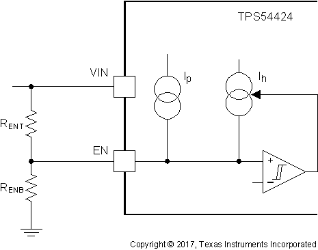 Figure 27. Adjustable UVLO Using EN

vertical spacer

7.3.7 Soft Start and Tracking
The TPS54424 regulates to the SS/TRK pin while its voltage is lower than the internal reference to implement soft start. A capacitor on the SS/TRK pin to ground sets the soft start time. The SS/TRK pin has an internal pull-up current source of 5 μA that charges the external soft start capacitor. Equation 4 calculates the required soft start capacitor value. The FB voltage will follow the SS/TRK pin voltage with a 25 mV offset up to 90% of the internal voltage reference. When the SS/TRK voltage is greater than 90% of the internal reference voltage the offset increases as the effective system reference transitions from the SS/TRK voltage to the internal voltage reference.

If during normal operation, VIN goes below the UVLO, EN pin pulled below 1.15 V, or a thermal shutdown event occurs, the TPS54424 stops switching and the SS/TRK pin floats. When the VIN goes above UVLO, EN goes above 1.20 V, or a thermal shutdown is exited, the SS/TRK pin is discharged to near ground before reinitiating a powering up sequence.
When the COMP pin voltage is clamped by the maximum COMP clamp in an overload condition the SS/TRK pin is discharged to near the FB voltage. When the overload condition is removed, the soft-start circuit controls the recovery from the fault output level to the nominal output regulation voltage. At the beginning of recovery a spike in the output voltage may occur while the COMP voltage transitions from the maximum clamp to the value determined by the loop.
7.3.8 Safe Start-up into Pre-Biased Outputs
The device has been designed to prevent the low-side MOSFET from discharging a pre-biased output. During monotonic pre-biased startup, the low-side MOSFET is not allowed to sink current until the SS/TRK pin voltage is higher than the FB pin voltage and the high-side MOSFET begins to switch. The one exception is if the BOOT-SW voltage is below the UVLO threshold. While in BOOT-SW UVLO, the low-side MOSFET is allowed to turn on to charge the BOOT capacitor. The low-side MOSFET reverse current protection provides another layer of protection for the device after the high-side MOSFET begins to switch.
7.3.9 Power Good
The PGOOD pin is an open-drain output requiring an external pull-up resistor to output a high signal. Once the FB pin is between 91% and 106% of the internal voltage reference and SS/TRK is greater than 0.75 V, after a 272 cycle deglitch time the PGOOD pin is de-asserted and the pin floats. A pull-up resistor between the values of 10 kΩ and 100 kΩ to a voltage source that is 6.5 V or less is recommended. PGOOD is in a defined state once the VIN input voltage is greater than 1 V but with reduced current sinking capability.
When the FB is lower than 89% or greater than 108% of the nominal internal reference voltage, after a 16 cycle deglitch time the PGOOD pin is pulled low. PGOOD is immediately pulled low if VIN falls below its UVLO, EN pin is pulled low or the TPS54424 enters thermal shutdown.
7.3.10 Sequencing (SS/TRK)
Many of the common power supply sequencing methods can be implemented using the SS/TRK, EN and PGOOD pins.
The sequential method is illustrated in Figure 28 using two TPS54424 or similar devices. The power good of the first device is coupled to the EN pin of the second device which enables the second power supply once the primary supply reaches regulation.
Figure 29 shows the method implementing ratiometric sequencing by connecting the SS/TRK pins of two devices together. The regulator outputs ramp up and reach regulation at the same time. When calculating the soft-start time the current source must be doubled in Equation 4.
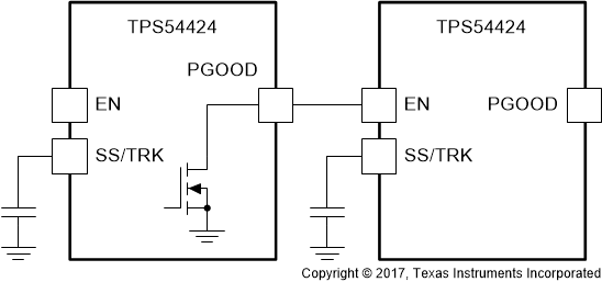 Figure 28. Sequential Start-Up Sequence
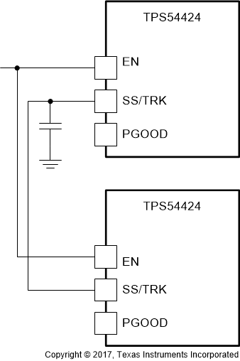 Figure 29. Ratiometric Start-Up Sequence
Ratiometric and simultaneous power supply sequencing can be implemented by connecting the resistor network of RTRT and RTRB shown in Figure 30 to the output of the power supply that needs to be tracked or another voltage reference source. Using Equation 6 and Equation 7, the tracking resistors can be calculated to initiate the VOUT2 slightly before, after or at the same time as VOUT1. Equation 5 is the voltage difference between VOUT1 and VOUT2.
To design a ratiometric start-up in which the VOUT2 voltage is slightly greater than the VOUT1 voltage when VOUT2 reaches regulation, use a negative number in Equation 6 and Equation 7 for deltaV. Equation 5 results in a positive number for applications where the VOUT2 is slightly lower than VOUT1 when VOUT2 regulation is achieved.
The deltaV variable is zero volts for simultaneous sequencing. To minimize the effect of the inherent SS/TRK to FB offset (Vssoffset = 25 mV) in the soft-start circuit and the offset created by the pull-up current source (Iss = 5 μA) and tracking resistors, the Vssoffset and Iss are included as variables in the equations.
To ensure proper operation of the device, the calculated RTRT value from Equation 6 must be greater than the value calculated in Equation 8.

vertical spacer

vertical spacer

vertical spacer

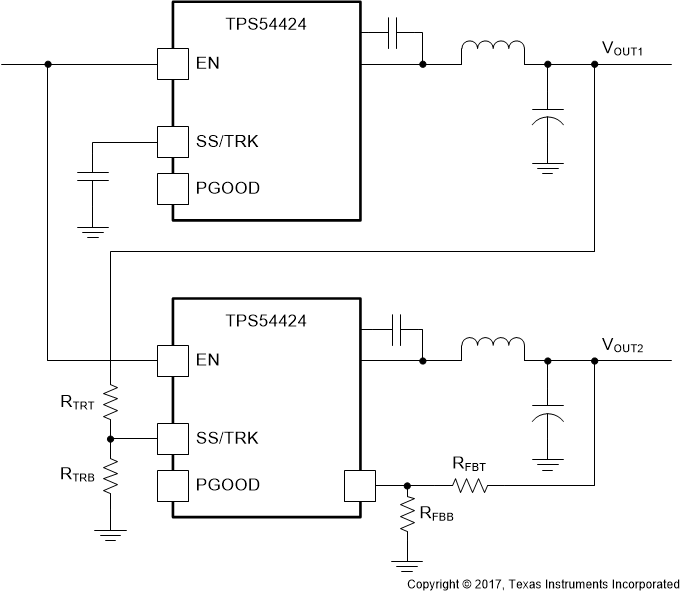 Figure 30. Ratiometric and Simultaneous Start-Up Sequence
7.3.11 Adjustable Switching Frequency (RT Mode)
In RT mode, a resistor (RT resistor) is connected between the RT/CLK pin and AGND. The switching frequency of the device is adjustable from 200 kHz to 1600 kHz by placing a maximum of 250 kΩ and minimum of 30.1 kΩ respectively. To determine the RT resistance for a given switching frequency, use Equation 9. To reduce the solution size one would set the switching frequency as high as possible, but tradeoffs of the supply efficiency and minimum controllable on-time should be considered. Equation 10 can be used to calculate the switching frequency for a given RT resistance.

vertical spacer

7.3.12 Synchronization (CLK Mode)
An internal Phase Locked Loop (PLL) has been implemented to allow synchronization from 200 kHz to 1600 kHz, and to easily switch from RT mode to CLK mode. To implement the synchronization feature, connect a square wave clock signal to the RT/CLK pin with a duty cycle from 20% to 80%. If the clock signals rising edge occurs near the falling edge of SW, increased SW jitter may occur. Use Equation 11 to calculate the maximum clock pulse width to minimize jitter in CLK mode. The clock signal amplitude must transition lower than 0.8 V and higher than 2 V. The start of the switching cycle is synchronized to the falling edge of the RT/CLK pin.

In applications where both RT mode and CLK mode are needed, the device can be configured as shown in Figure 31. Before the external clock is present, the device works in RT mode and the switching frequency is set by RT resistor. When the external clock is present, the CLK mode overrides the RT mode. The first time the SYNC pin is pulled above the RT/CLK high threshold (2 V), the device switches from the RT mode to the CLK mode and the RT/CLK pin becomes high impedance as the PLL starts to lock onto the frequency of the external clock.
If the input clock goes away the internal clock frequency begins to drop and after 10 µs without a clock the device returns to RT mode. Output undershoot while the switching frequency drops can occur. Output overshoot can also occur when the switching frequency steps back up to the RT mode frequency. A high impedance tri-state buffer as shown in Figure 33 is recommended for best performance during the transition from CLK mode to RT mode because it minimizes the loading on the RT/CLK pin allowing faster transition back to RT mode. Figure 34 shows the typical performance for the transition from RT mode to CLK mode then back to RT mode.
A series RC circuit as shown in Figure 32 can also be used to interface the RT/CLK pin but the capacitive load slows down the transition back to RT mode. The series RC circuit is not recommended if the transition from CLK mode to RT mode is important. A capacitor in the range of 47 pF to 470 pF is recommended. When using the series RC circuit verify the amplitude of the signal at the RT/CLK pin goes above the high threshold.
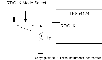 Figure 31. Simplified Circuit When Using Both RT Mode and CLK Mode
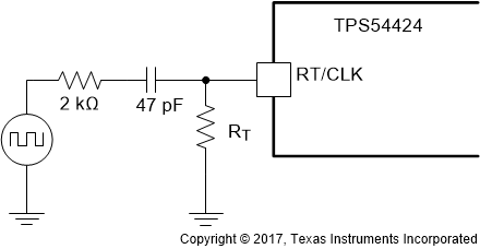 Figure 32. Interfacing to the RT/CLK Pin with Series RC
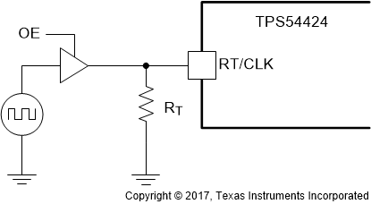 Figure 33. Interfacing to the RT/CLK Pin with Buffer
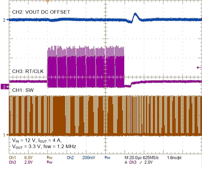 Figure 34. RT to CLK to RT Transition with Buffer
7.3.13 Bootstrap Voltage and 100% Duty Cycle Operation (BOOT)
The device provides an integrated bootstrap voltage regulator. A small capacitor between the BOOT and SW pins provides the gate drive voltage for the high side MOSFET. The BOOT capacitor is refreshed when the low-side MOSFET is on. The recommended value of the BOOT capacitor is 0.1 μF. A ceramic capacitor with an X7R or X5R grade dielectric with a voltage rating of 10 V or higher is recommended for stable performance over temperature and voltage.
When operating with a low voltage difference from input to output, the high side MOSFET of the device will operate at 100% duty cycle as long as the BOOT to SW pin voltage is greater than 2.2 V. The device will begin to transition to 100% duty cycle operation when the high-side MOSFET off-time is less than 200 ns typical. When the voltage from BOOT to SW drops below 2.2 V, the high-side MOSFET is turned off due to BOOT UVLO and the low side MOSFET pulls SW low to recharge the BOOT capacitor. When operating at 100% duty cycle the high-side MOSFET can remain on for many switching cycles before the MOSFET is turned off to refresh the capacitor because the gate drive current sourced by the BOOT capacitor is small. The effective switching frequency reduced and the effective maximum duty cycle of the switching regulator is near 100%. The output voltage of the converter during dropout is mainly influenced by the voltage drops across the power MOSFET, the inductor resistance, and the printed circuit board resistance.
7.3.14 Output Overvoltage Protection (OVP)
The TPS54424 incorporates an output overvoltage protection (OVP) circuit to minimize output voltage overshoot. The OVP feature minimizes the overshoot by comparing the FB pin voltage to the OVP threshold. The OVP threshold is the same as the 108% PGOOD threshold. If the FB pin voltage is greater than the OVP threshold the high-side MOSFET is turned off preventing current from flowing to the output and minimizing output overshoot. When the high-side MOSFET turns off, the low-side MOSFET turns on and the current in the inductor discharges. The output voltage can overshoot the OVP threshold as the current in the inductor discharges to 0 A. When the FB voltage drops lower than the 106% PGOOD threshold, the high-side MOSFET is allowed to turn on at the next clock cycle.
7.3.15 Overcurrent Protection
The device is protected from overcurrent conditions by cycle-by-cycle current limiting on both the high-side MOSFET and the low-side MOSFET. In an extended overcurrent condition the device will enter hiccup to reduce power dissipation.
7.3.15.1 High-side MOSFET Overcurrent Protection
The device implements current mode control which uses the COMP pin voltage to control the turnoff of the high-side MOSFET and the turnon of the low-side MOSFET on a cycle-by-cycle basis. Each cycle the switch current and the current reference generated by the COMP pin voltage are compared, when the peak switch current intersects the current reference the high-side switch is turned off. The maximum peak switch current through the high-side MOSFET for overcurrent protection is done by limiting the current reference internally. If the peak current required to regulate the output is greater than the internal limit, the output voltage is pulled low and the error amplifier responds by driving the COMP pin high. The maximum COMP voltage is then clamped by an internal COMP clamp circuit. If the COMP voltage is clamped high for more than the hiccup wait time of 512 switching cycles, the device will shut down itself and restart after the hiccup time of 16384 cycles.
7.3.15.2 Low-side MOSFET Overcurrent Protection
While the low-side MOSFET is turned on the current through it is monitored. During normal operation the low-side MOSFET sources current to the load. At the end of every clock cycle, the low-side MOSFET sourcing current is compared to the internally set low-side sourcing current limit. If the low-side sourcing current is exceeded the high-side MOSFET is not turned on and the low-side MOSFET stays on for the next cycle. The high-side MOSFET is turned on again when the low-side current is below the low-side sourcing current limit at the start of a cycle. The low-side sourcing current limit prevents current runaway.
The low-side MOSFET may also sink current from the load. If the low-side sinking current limit is exceeded the low-side MOSFET is turned off immediately for the rest of that clock cycle. In this scenario both MOSFETs are off until the start of the next cycle. If the low-side MOSFET turns off due to sinking current limit protection, the low-side MOSFET can only turn on again after the high-side MOSFET turns on then off or if the device enters BOOT UVLO.
7.4 Device Functional Modes
The EN pin and a VIN UVLO is used to control turn on and turn off of the TPS54424. The device becomes active when V(VIN) exceeds the 4.1 V typical UVLO and when V(EN) exceeds 1.20 V typical. The EN pin has an internal current source to enable the output when the EN pin is left floating. If the EN pin is pulled low the device is put into a low quiescent current state.