JAJSLN5B May 2012 – April 2021 TPS54525
PRODUCTION DATA
- 1 特長
- 2 アプリケーション
- 3 概要
- 4 Revision History
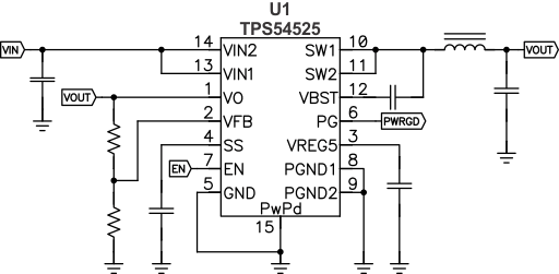
- 5 Pin Configuration and Functions
- 6 Specifications
- 7 Detailed Description
- 8 Application and Implementation
- 9 Power Supply Recommendations
- 10Layout
- 11Device and Documentation Support
パッケージ・オプション
メカニカル・データ(パッケージ|ピン)
- PWP|14
サーマルパッド・メカニカル・データ
- PWP|14
発注情報
3 概要
TPS54525 は、適応型オン時間、D-CAP2™ モードの同期整流式降圧コンバータです。このデバイスを採用することで、各種機器の電源バス・レギュレータに対して、コスト効果が高く、部品数の少ない、低スタンバイ電流のソリューションを実現できます。本デバイスの主制御ループは、外部補償部品なしで非常に高速な過渡応答が得られる D-CAP2™ モード制御を使用しています。また、低 ESR (等価直列抵抗) の出力コンデンサ (例:POSCAP、SP-CAP) と超低 ESR セラミック・コンデンサの両方をサポートできる独自の回路も備えています。このデバイスは、4.5V~18V の VIN 入力で動作します。出力電圧は、0.76V~5.5V の範囲でプログラミングできます。また、調整可能なソフト・スタート時間とパワー・グッド機能も備えています。TPS54525 は 14 ピンの HTSSOP パッケージで供給され、–40℃~85℃の温度範囲で動作するよう設計されています。
製品情報
| 部品番号 | パッケージ | 本体サイズ |
|---|---|---|
| TPS54525 | HTSSOP | 5.00mm × 6.40mm |