JAJSJP2A September 2020 – August 2021 TPS54618C-Q1
PRODUCTION DATA
- 1 特長
- 2 アプリケーション
- 3 概要
- 4 Revision History
- 5 Pin Configuration and Functions
- 6 Specifications
-
7 Detailed Description
- 7.1 Overview
- 7.2 Functional Block Diagram
- 7.3
Feature Description
- 7.3.1 Fixed Frequency PWM Control
- 7.3.2 Slope Compensation and Output Current
- 7.3.3 Bootstrap Voltage (Boot) and Low Dropout Operation
- 7.3.4 Error Amplifier
- 7.3.5 Voltage Reference
- 7.3.6 Adjusting the Output Voltage
- 7.3.7 Enable and Adjusting Undervoltage Lockout
- 7.3.8 Soft-Start Pin
- 7.3.9 Sequencing
- 7.3.10 Constant Switching Frequency and Timing Resistor (RT/CLK Pin)
- 7.3.11 Overcurrent Protection
- 7.3.12 Frequency Shift
- 7.3.13 Reverse Overcurrent Protection
- 7.3.14 Synchronize Using the RT/CLK Pin
- 7.3.15 Power Good (PWRGD Pin)
- 7.3.16 Overvoltage Transient Protection
- 7.3.17 Thermal Shutdown
- 7.4 Device Functional Modes
-
8 Application and Implementation
- 8.1 Application Information
- 8.2
Typical Application
- 8.2.1 Design Requirements
- 8.2.2
Detailed Design Procedure
- 8.2.2.1 Step One: Select the Switching Frequency
- 8.2.2.2 Step Two: Select the Output Inductor
- 8.2.2.3 Step Three: Choose the Output Capacitor
- 8.2.2.4 Step Four: Select the Input Capacitor
- 8.2.2.5 Step Five: Choose the Soft-Start Capacitor
- 8.2.2.6 Step Six: Select the Bootstrap Capacitor
- 8.2.2.7 Step Eight: Select Output Voltage and Feedback Resistors
- 8.2.2.8 Step Nine: Select Loop Compensation Components
- 8.2.3 Application Curves
- 9 Power Supply Recommendations
- 10Layout
- 11Device and Documentation Support
- 12Mechanical, Packaging, and Orderable Information
パッケージ・オプション
メカニカル・データ(パッケージ|ピン)
- RTE|16
サーマルパッド・メカニカル・データ
- RTE|16
発注情報
7.3.9 Sequencing
Many of the common power supply sequencing methods can be implemented using the SS/TR, EN, and PWRGD pins. The sequential method can be implemented using an open-drain or collector output of a power-on reset pin of another device. Figure 7-3 shows the sequential method. The power good is coupled to the EN pin on the TPS54618C-Q1 which enables the second power supply once the primary supply reaches regulation.
Ratio-metric start-up can be accomplished by connecting the SS/TR pins together. The regulator outputs ramp up and reach regulation at the same time. When calculating the slow-start time, the pullup current source must be doubled in Equation 4. The ratio-metric method is shown in Figure 7-5.

 Figure 7-4 Sequential Start-Up
 Using EN and PWRGD
 Figure 7-5 Schematic for Ratio-Metric Start-Up Sequence
Ratio-metric and simultaneous power supply sequencing can be implemented by connecting the resistor network of R1 and R2 shown in Figure 7-7 to the output of the power supply that needs to be tracked or another voltage reference source. Using Equation 5 and Equation 6, the tracking resistors can be calculated to initiate the Vout2 slightly before, after, or at the same time as Vout1. Equation 7 is the voltage difference between Vout1 and Vout2. The ΔV variable is zero volts for simultaneous sequencing. To minimize the effect of the inherent SS/TR to VSENSE offset (Vssoffset) in the slow-start circuit and the offset created by the pullup current source (Iss) and tracking resistors, the Vssoffset and Iss are included as variables in the equations. To design a ratio-metric start-up in which the Vout2 voltage is slightly greater than the Vout1 voltage when Vout2 reaches regulation, use a negative number in Equation 5 through Equation 7 for ΔV. Equation 7 results in a positive number for applications which the Vout2 is slightly lower than Vout1 when Vout2 regulation is achieved. Because the SS/TR pin must be pulled below 40 mV before starting after an EN, UVLO, or thermal shutdown fault, careful selection of the tracking resistors is needed to ensure the device restarts after a fault. Make sure the calculated R1 value from Equation 5 is greater than the value calculated in Equation 8 to ensure the device can recover from a fault. As the SS/TR voltage becomes more than 85% of the nominal reference voltage the Vssoffset becomes larger as the slow-start circuits gradually handoff the regulation reference to the internal voltage reference. The SS/TR pin voltage needs to be greater than 1.1 V for a complete hand off to the internal voltage reference as shown in Figure 7-6.
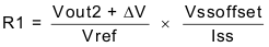
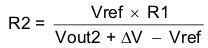
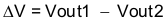
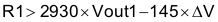
 Figure 7-7 Ratio-Metric and Simultaneous Start-Up Sequence