JAJSMU6C June 2012 – September 2021 TPS54719
PRODUCTION DATA
- 1 特長
- 2 アプリケーション
- 3 概要
- 4 Revision History
- 5 Pin Configuration and Functions
- 6 Specifications
-
7 Detailed Description
- 7.1 Overview
- 7.2 Functional Block Diagram
- 7.3
Feature Description
- 7.3.1 Fixed Frequency PWM Control
- 7.3.2 Slope Compensation And Output Current
- 7.3.3 Bootstrap Voltage (Boot) And Low Dropout Operation
- 7.3.4 Error Amplifier
- 7.3.5 Voltage Reference
- 7.3.6 Adjusting The Output Voltage
- 7.3.7 Enable and Adjusting Undervoltage Lockout
- 7.3.8 Slow Start/Tracking Pin
- 7.3.9 Sequencing
- 7.4
Device Functional Modes
- 7.4.1 Constant Switching Frequency And Timing Resistor (RT Pin)
- 7.4.2 Overcurrent Protection
- 7.4.3 Frequency Shift
- 7.4.4 Reverse Overcurrent Protection
- 7.4.5 Power Good (PWRGD Pin)
- 7.4.6 Overvoltage Transient Protection
- 7.4.7 Thermal Shutdown
- 7.4.8 Small Signal Model For Loop Response
- 7.4.9 Simple Small Signal Model For Peak Current Mode Control
- 7.4.10 Small Signal Model For Frequency Compensation
-
8 Application and Implementation
- 8.1 Application Information
- 8.2
Typical Application
- 8.2.1 High Frequency, 1.8-V Output Power Supply Design With Adjusted UVLO
- 8.2.2 Design Requirements
- 8.2.3
Detailed Design Procedure
- 8.2.3.1 Selecting The Switching Frequency
- 8.2.3.2 Output Inductor Selection
- 8.2.3.3 Output Capacitor
- 8.2.3.4 Input Capacitor
- 8.2.3.5 Slow-Start Capacitor
- 8.2.3.6 Bootstrap Capacitor Selection
- 8.2.3.7 Undervoltage Lockout Set Point
- 8.2.3.8 Output Voltage And Feedback Resistors Selection
- 8.2.3.9 Compensation
- 8.2.4 Application Curves
- 9 Power Supply Recommendations
- 10Layout
- 11Device and Documentation Support
- 12Mechanical, Packaging, and Orderable Information
パッケージ・オプション
メカニカル・データ(パッケージ|ピン)
- RTE|16
サーマルパッド・メカニカル・データ
- RTE|16
発注情報
6.7 Typical Characteristics
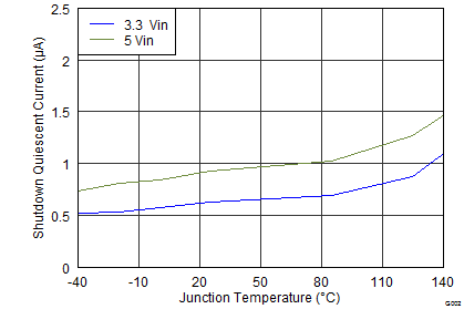 Figure 6-1 Shutdown Supply Current vs Temperature
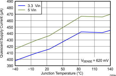 Figure 6-3 VIN Supply Current vs Temperature
 Figure 6-5 UVLO Threshold vs Temperature
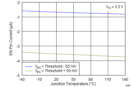 Figure 6-7 EN Pin Current vs Temperature
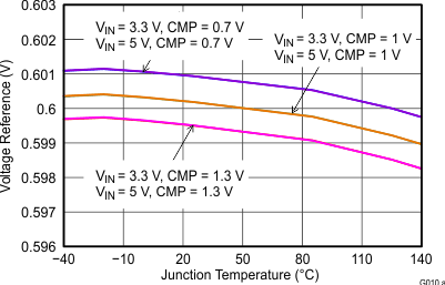 Figure 6-9 Voltage Reference vs Temperature
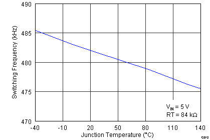 Figure 6-11 Switching Frequency vs Temperature
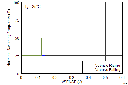 Figure 6-13 Switching Frequency vs Vsense
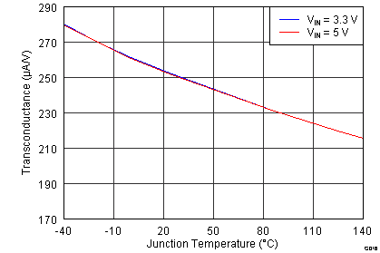 Figure 6-15 Transconductance vs Temperature
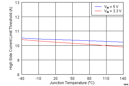 Figure 6-17 High-Side FET Current Limit vs Temperature
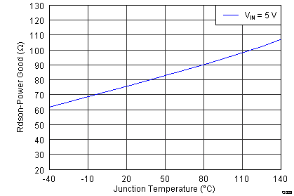 Figure 6-19 PWRGD Rdson vs Temperature
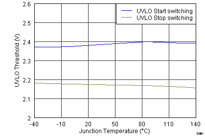 Figure 6-21 UVLO Threshold vs Temperature
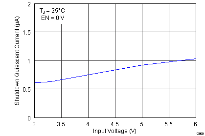 Figure 6-2 Shutdown Supply Current vs Voltage
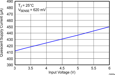 Figure 6-4 VIN Supply
Current vs Voltage
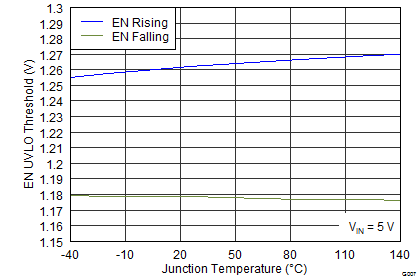 Figure 6-6 UVLO Threshold vs Temperature
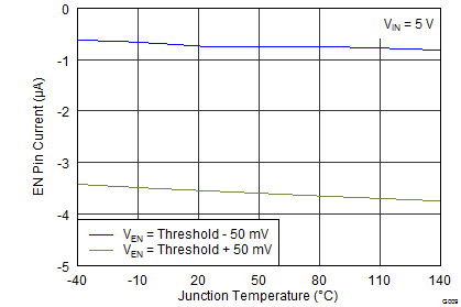 Figure 6-8 EN Pin Current vs Temperature
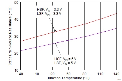 Figure 6-10 Rdson vs Temperature
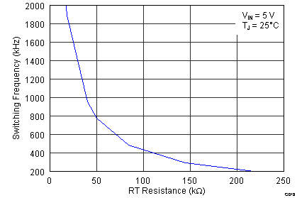 Figure 6-12 Switching Frequency vs RT Resistance
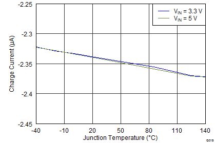 Figure 6-14 SS Charge Current vs Temperature
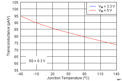 Figure 6-16 Transconductance (Slow Start) vs Temperature
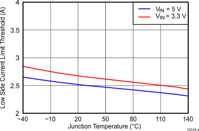 Figure 6-18 Low-Side FET Current Limit vs Temperature
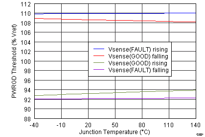 Figure 6-20 PWRGD Threshold vs Temperature