JAJSIT5D March 2020 – July 2021 TPS548A29
PRODUCTION DATA
- 1 特長
- 2 アプリケーション
- 3 概要
- 4 Revision History
- 5 Pin Configuration and Functions
- 6 Specifications
-
7 Detailed Description
- 7.1 Overview
- 7.2 Functional Block Diagram
- 7.3
Feature Description
- 7.3.1 Internal VCC LDO And Using External Bias On VCC Pin
- 7.3.2 Enable
- 7.3.3 Output Voltage Setting
- 7.3.4 Internal Fixed Soft Start and External Adjustable Soft Start
- 7.3.5 External REFIN For Output Voltage Tracking
- 7.3.6 Frequency and Operation Mode Selection
- 7.3.7 D-CAP3 Control
- 7.3.8 Low-side FET Zero-Crossing
- 7.3.9 Current Sense and Positive Overcurrent Protection
- 7.3.10 Low-side FET Negative Current Limit
- 7.3.11 Power Good
- 7.3.12 Overvoltage and Undervoltage Protection
- 7.3.13 Out-Of-Bounds (OOB) Operation
- 7.3.14 Output Voltage Discharge
- 7.3.15 UVLO Protection
- 7.3.16 Thermal Shutdown
- 7.4 Device Functional Modes
-
8 Application and Implementation
- 8.1 Application Information
- 8.2
Typical Application
- 8.2.1 Design Requirements
- 8.2.2
Detailed Design Procedure
- 8.2.2.1 Output Voltage Setting Point
- 8.2.2.2 Choose the Switching Frequency and the Operation Mode
- 8.2.2.3 Choose the Inductor
- 8.2.2.4 Set the Current Limit (TRIP)
- 8.2.2.5 Choose the Output Capacitor
- 8.2.2.6 Choose the Input Capacitors (CIN)
- 8.2.2.7 Soft Start Capacitor (SS/REFIN Pin)
- 8.2.2.8 EN Pin Resistor Divider
- 8.2.2.9 VCC Bypass Capacitor
- 8.2.2.10 BOOT Capacitor
- 8.2.2.11 PGOOD Pullup Resistor
- 8.2.3 Application Curves
- 9 Power Supply Recommendations
- 10Layout
- 11Device and Documentation Support
- 12Mechanical, Packaging, and Orderable Information
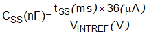
7.3.4 Internal Fixed Soft Start and External Adjustable Soft Start
The TPS548A29 implements a circuit to allow both internal fixed soft start and external adjustable soft start. The internal soft-start time is typically 1.5 ms. The soft-start time can be increased by adding a soft-start (SS) capacitor between the SS/REFIN and VSNS– pins. The total SS capacitor value can be determined by Equation 2. The device follows the longer SS ramp among the internal SS time and the SS time determined by the external SS capacitors. The recommended maximum SS capacitor is 1 µF. A minimum 1-nF SS capacitor is required.
The device does not require a capacitor from the SS/REFIN pin to AGND, thus it is not recommenced to place a capacitor from the SS/REFIN pin to AGND. If both CSS/REFIN-to-VSNS– and CSS/REFIN-to-AGND capacitors exist, place CSS/REFIN-to-VSNS– more closely with shortest trace back to the VSNS– pin.
The SS/REFIN pin is discharged internally during the internal power-on delay to make sure the soft-start ramp always starts from zero.