JAJSDT2A August 2016 – September 2017 TPS549D22
PRODUCTION DATA.
- 1 特長
- 2 アプリケーション
- 3 概要
- 4 改訂履歴
- 5 Pin Configuration and Functions
- 6 Specifications
-
7 Detailed Description
- 7.1 Overview
- 7.2 Functional Block Diagram
- 7.3 Feature Description
- 7.4 Device Functional Modes
- 7.5
Programming
- 7.5.1 Programmable Pin-Strap Settings
- 7.5.2 Programmable Analog Configurations
- 7.5.3 PMBus Programming
- 7.5.4
Register Maps
- 7.5.4.1 OPERATION Register (address = 1h)
- 7.5.4.2 ON_OFF_CONFIG Register (address = 2h)
- 7.5.4.3 CLEAR FAULTS (address = 3h)
- 7.5.4.4 WRITE PROTECT (address = 10h)
- 7.5.4.5 STORE_DEFAULT_ALL (address = 11h)
- 7.5.4.6 RESTORE_DEFAULT_ALL (address = 12h)
- 7.5.4.7 CAPABILITY (address = 19h)
- 7.5.4.8 VOUT_MODE (address = 20h)
- 7.5.4.9 VOUT_COMMAND (address = 21h)
- 7.5.4.10 VOUT_MARGIN_HIGH (address = 25h)
- 7.5.4.11 VOUT_MARGIN_LOW (address = 26h)
- 7.5.4.12 STATUS_BYTE (address = 78h)
- 7.5.4.13 STATUS_WORD (High Byte) (address = 79h)
- 7.5.4.14 STATUS_VOUT (address = 7Ah)
- 7.5.4.15 STATUS_IOUT (address = 7Bh)
- 7.5.4.16 STATUS_CML (address = 7Eh)
- 7.5.4.17 MFR_SPECIFIC_00 (address = D0h)
- 7.5.4.18 MFR_SPECIFIC_01 (address = D1h)
- 7.5.4.19 MFR_SPECIFIC_02 (address = D2h)
- 7.5.4.20 MFR_SPECIFIC_03 (address = D3h)
- 7.5.4.21 MFR_SPECIFIC_04 (address = D4h)
- 7.5.4.22 MFR_SPECIFIC_06 (address = D6h)
- 7.5.4.23 MFR_SPECIFIC_07 (address = D7h)
- 7.5.4.24 MFR_SPECIFIC_44 (address = FCh)
-
8 Application and Implementation
- 8.1 Application Information
- 8.2
Typical Application: TPS549D22 1.5-V to 16-V Input, 1-V Output, 40-A Converter
- 8.2.1 Design Requirements
- 8.2.2
Detailed Design Procedure
- 8.2.2.1 Custom Design With WEBENCH® Tools
- 8.2.2.2 Switching Frequency Selection
- 8.2.2.3 Inductor Selection
- 8.2.2.4 Output Capacitor Selection
- 8.2.2.5 Input Capacitor Selection
- 8.2.2.6 Bootstrap Capacitor Selection
- 8.2.2.7 BP Pin
- 8.2.2.8 R-C Snubber and VIN Pin High-Frequency Bypass
- 8.2.2.9 Optimize Reference Voltage (VSEL)
- 8.2.2.10 MODE Pin Selection
- 8.2.2.11 ADDR Pin Selection
- 8.2.2.12 Overcurrent Limit Design
- 8.2.3 Application Curves
- 9 Power Supply Recommendations
- 10Layout
- 11デバイスおよびドキュメントのサポート
- 12メカニカル、パッケージ、および注文情報
- 13Package Option Addendum
6 Specifications
6.1 Absolute Maximum Ratings
over operating free-air temperature range (unless otherwise noted) (1)(2)| MIN | MAX | UNIT | |||
|---|---|---|---|---|---|
| Input voltage | PVIN | –0.3 | 25 | V | |
| VDD | –0.3 | 25 | |||
| BOOT | –0.3 | 34 | |||
| BOOT to SW | DC | –0.3 | 7.7 | ||
| < 10 ns | –0.3 | 9.0 | |||
| PMB_CLK, PMB_DATA | –0.3 | 6 | |||
| EN_UVLO, VOSNS, MODE, ADDR, ILIM | –0.3 | 7.7 | |||
| RSP, RESV_TRK, VSEL | –0.3 | 3.6 | |||
| RSN | –0.3 | 0.3 | |||
| PGND, AGND, DRGND | –0.3 | 0.3 | |||
| SW | DC | –0.3 | 25 | ||
| < 10 ns | –5 | 27 | |||
| Output voltage | PGOOD, BP | –0.3 | 7.7 | V | |
| Output voltage | SMB_ALRT#, PMB_DATA | –0.3 | 6 | V | |
| Junction temperature, TJ | –55 | 150 | °C | ||
| Storage temperature, Tstg | –55 | 150 | °C | ||
(1) Stresses beyond those listed under Absolute Maximum Ratings may cause permanent damage to the device. These are stress ratings only, which do not imply functional operation of the device at these or any other conditions beyond those indicated under Recommended Operating Conditions. Exposure to absolute-maximum-rated conditions for extended periods may affect device reliability.
(2) All voltage values are with respect to the network ground terminal unless otherwise noted.
6.2 ESD Ratings
| VALUE | UNIT | |||
|---|---|---|---|---|
| V(ESD) | Electrostatic discharge | Human-body model (HBM), per ANSI/ESDA/JEDEC JS-001(1) | ±2000 | V |
| Charged-device model (CDM), per JEDEC specification JESD22-C101(2) | ±500 | |||
(1) JEDEC document JEP155 states that 500-V HBM allows safe manufacturing with a standard ESD control process.
(2) JEDEC document JEP157 states that 250-V CDM allows safe manufacturing with a standard ESD control process.
6.3 Recommended Operating Conditions
over operating free-air temperature range (unless otherwise noted)| MIN | MAX | UNIT | |||
|---|---|---|---|---|---|
| Input voltage | PVIN | 1.5 | 16 | V | |
| VDD | 4.5 | 22 | |||
| BOOT | –0.1 | 24.5 | |||
| BOOT to SW | DC | –0.1 | 6.5 | ||
| < 10 ns | –0.1 | 7 | |||
| PMB_CLK, PMB_DATA | –0.1 | 5.5 | |||
| EN_UVLO, VOSNS, MODE, ADDR, ILIM | –0.1 | 5.5 | |||
| RSP, RESV_TRK, VSEL | –0.1 | 3.3 | |||
| RSN | –0.1 | 0.1 | |||
| PGND, AGND, DRGND | –0.1 | 0.1 | |||
| SW | DC | –0.1 | 18 | ||
| < 10 ns | –5 | 27 | |||
| Output voltage | PGOOD, BP | –0.1 | 7 | V | |
| Output voltage | SMB_ALRT#, PMB_DATA | –0.1 | 5.5 | V | |
| Junction temperature, TJ | –40 | 125 | °C | ||
6.4 Thermal Information
| THERMAL METRIC(1) | TPS549D22 | UNIT | |
|---|---|---|---|
| RVF (LQFN-CLIP) | |||
| (40 PINS) | |||
| RθJA | Junction-to-ambient thermal resistance | 28.5 | °C/W |
| RθJC(top) | Junction-to-case (top) thermal resistance | 18.3 | °C/W |
| RθJB | Junction-to-board thermal resistance | 3.6 | °C/W |
| ψJT | Junction-to-top characterization parameter | 0.96 | °C/W |
| ψJB | Junction-to-board characterization parameter | 3.6 | °C/W |
| RθJC(bot) | Junction-to-case (bottom) thermal resistance | 0.6 | °C/W |
(1) For more information about traditional and new thermal metrics, see the Semiconductor and IC Package Thermal Metrics application report.
6.5 Electrical Characteristics
over operating free-air temperature range, VVDD = 12 V, VEN_UVLO = 5 V (unless otherwise noted)| PARAMETER | TEST CONDITION | MIN | TYP | MAX | UNIT | ||
|---|---|---|---|---|---|---|---|
| MOSFET ON-RESISTANCE (RDS(on)) | |||||||
| RDS(on) | High-side FET | (VBOOT – VSW) = 5 V, ID = 25 A, TJ = 25°C | 2.9 | mΩ | |||
| Low-side FET | VVDD = 5 V, ID = 25 A, TJ = 25°C | 1.2 | mΩ | ||||
| INPUT SUPPLY AND CURRENT | |||||||
| VVDD | VDD supply voltage | Nominal VDD voltage range | 4.5 | 22 | V | ||
| IVDD | VDD bias current | No load, power conversion enabled (no switching), TA = 25°C, | 2 | mA | |||
| IVDDSTBY | VDD standby current | No load, power conversion disabled, TA = 25°C | 700 | µA | |||
| UNDERVOLTAGE LOCKOUT | |||||||
| VVDD_UVLO | VDD UVLO rising threshold | 4.23 | 4.25 | 4.34 | V | ||
| VVDD_UVLO(HYS) | VDD UVLO hysteresis | 0.2 | V | ||||
| VEN_ON_TH | EN_UVLO on threshold | 1.45 | 1.6 | 1.75 | V | ||
| VEN_HYS | EN_UVLO hysteresis | 270 | 300 | 340 | mV | ||
| IEN_LKG | EN_UVLO input leakage current | VEN_UVLO = 5 V | –1 | 0 | 1 | µA | |
| INTERNAL REFERENCE VOLTAGE AND RANGE | |||||||
| VINTREF | Internal REF voltage | 900.4 | mV | ||||
| VINTREFTOL | Internal REF voltage tolerance | –40°C ≤ TJ ≤ 125°C | –0.5% | 0.5% | |||
| VINTREF | Internal REF voltage range | 0.6 | 1.2 | V | |||
| OUTPUT VOLTAGE | |||||||
| VIOS_LPCMP | Loop comparator input offset voltage(1) | –2.5 | 2.5 | mV | |||
| IRSP | RSP input current | VRSP = 600 mV | –1 | 1 | µA | ||
| IVO(dis) | VO discharge current | VVO = 0.5 V, power conversion disabled | 8 | 12 | mA | ||
| DIFFERENTIAL REMOTE SENSE AMPLIFIER | |||||||
| fUGBW | Unity gain bandwidth(1) | 5 | 7 | MHz | |||
| A0 | Open loop gain(1) | 75 | dB | ||||
| SR | Slew rate(1) | ±4.7 | V/µsec | ||||
| VIRNG | Input range(1) | –0.2 | 1.8 | V | |||
| VOFFSET | Input offset voltage(1) | –3.5 | 3.5 | mV | |||
| INTERNAL BOOT STRAP SWITCH | |||||||
| VF | Forward voltage | VBP-BOOT, IF = 10 mA, TA = 25°C | 0.1 | 0.2 | V | ||
| IBOOT | VBST leakage current | VBOOT = 30 V, VSW = 25 V, TA = 25°C | 0.01 | 1.5 | µA | ||
| SWITCHING FREQUENCY | |||||||
| fSW | VO switching frequency(2) | VIN = 12 V, VVO = 1 V, TA = 25°C | 275 | 315 | 350 | kHz | |
| 380 | 425 | 475 | |||||
| 490 | 550 | 615 | |||||
| 585 | 650 | 740 | |||||
| 740 | 825 | 930 | |||||
| 790 | 900 | 995 | |||||
| 920 | 1025 | 1160 | |||||
| 950 | 1125 | 1250 | |||||
| tON(min) | Minimum on time(1) | 60 | ns | ||||
| tOFF(min) | Minimum off time(1) | DRVH falling to rising | 300 | ns | |||
| MODE, VSEL, ADDR DETECTION | |||||||
| VDETECT_TH | MODE, VSEL, and ADDR detection voltage | VBP = 2.93 V, RHIGH = 100 kΩ |
Open | VBP | V | ||
| RLOW = 187 kΩ | 1.9091 | ||||||
| RLOW = 165 kΩ | 1.8243 | ||||||
| RLOW = 147 kΩ | 1.7438 | ||||||
| RLOW = 133 kΩ | 1.6725 | ||||||
| RLOW = 121 kΩ | 1.6042 | ||||||
| RLOW = 110 kΩ | 1.5348 | ||||||
| RLOW = 100 kΩ | 1.465 | ||||||
| RLOW = 90.9 kΩ | 1.3952 | ||||||
| RLOW = 82.5 kΩ | 1.3245 | ||||||
| RLOW = 75 kΩ | 1.2557 | ||||||
| RLOW = 68.1 kΩ | 1.187 | ||||||
| RLOW = 60.4 kΩ | 1.1033 | ||||||
| RLOW = 53.6 kΩ | 1.0224 | ||||||
| RLOW = 47.5 kΩ | 0.9436 | ||||||
| RLOW = 42.2 kΩ | 0.8695 | ||||||
| RLOW = 37.4 kΩ | 0.7975 | ||||||
| RLOW = 33.2 kΩ | 0.7303 | ||||||
| RLOW = 29.4 kΩ | 0.6657 | ||||||
| RLOW = 25.5 kΩ | 0.5953 | ||||||
| RLOW = 22.1 kΩ | 0.5303 | ||||||
| RLOW = 19.1 kΩ | 0.4699 | ||||||
| RLOW = 16.5 kΩ | 0.415 | ||||||
| RLOW = 14.3 kΩ | 0.3666 | ||||||
| RLOW = 12.1 kΩ | 0.3163 | ||||||
| RLOW = 10 kΩ | 0.2664 | ||||||
| RLOW = 7.87 kΩ | 0.2138 | ||||||
| RLOW = 6.19 kΩ | 0.1708 | ||||||
| RLOW = 4.64 kΩ | 0.1299 | ||||||
| RLOW = 3.16 kΩ | 0.0898 | ||||||
| RLOW = 1.78 kΩ | 0.0512 | ||||||
| RLOW = 0 Ω | GND | ||||||
| SOFT START | |||||||
| tSS | Soft-start time | VOUT rising from 0 V to 95% of final set point, RMODE_HIGH = 100 kΩ | RMODE_LOW = 60.4 kΩ | 7 | 8(3) | 10 | ms |
| RMODE_LOW = 53.6 kΩ | 3.6 | 4(4) | 5.2 | ||||
| RMODE_LOW = 47.5 kΩ | 1.6 | 2 | 2.8 | ||||
| RMODE_LOW = 42.2 kΩ | 0.8 | 1 | 1.6 | ||||
| POWER-ON DELAY | |||||||
| tPODLY | Power-on delay time | Delay from enable to switching POD[2:0] = 000 | 256 | µs | |||
| Delay from enable to switching POD[2:0] = 001 | 512 | ||||||
| Delay from enable to switching POD[2:0] = 010 | 1.024 | ms | |||||
| Delay from enable to switching POD[2:0] = 011 | 2.048 | ||||||
| Delay from enable to switching POD[2:0] = 100 | 4.096 | ||||||
| Delay from enable to switching POD[2:0] = 101 | 8.192 | ||||||
| Delay from enable to switching POD[2:0] = 110 | 16.384 | ||||||
| Delay from enable to switching POD[2:0] = 111 | 32.768 | ||||||
| PGOOD COMPARATOR | |||||||
| VPGTH | PGOOD threshold | PGOOD in from higher | 105 | 108 | 111 | %VREF | |
| PGOOD in from lower | 89 | 92 | 95 | ||||
| PGOOD out to higher | 120 | ||||||
| PGOOD out to lower | 68 | ||||||
| IPG | PGOOD sink current | VPGOOD = 0.5 V | 6.9 | mA | |||
| tPGDLY | PGOOD delay time | Delay for PGOOD going in, PGD[2:0] = 000 | 256 | µs | |||
| Delay for PGOOD going in, PGD[2:0] = 001 | 512 | ||||||
| Delay for PGOOD going in, PGD[2:0] = 010 | 1.024 | ms | |||||
| Delay for PGOOD going in, PGD[2:0] = 011 | 2.048 | ||||||
| Delay for PGOOD going in, PGD[2:0] = 100 | 4.096 | ||||||
| Delay for PGOOD going in, PGD[2:0] = 101 | 8.192 | ||||||
| Delay for PGOOD going in, PGD[2:0] = 110 | 16.384 | ||||||
| Delay for PGOOD going in, PGD[2:0] = 111 | 131 | ||||||
| Delay for PGOOD coming out | 2 | µs | |||||
| IPGLK | PGOOD leakage current | VPGOOD = 5 V | –1 | 0 | 1 | μA | |
| CURRENT DETECTION | |||||||
| VILM | VILIM voltage range | On-resistance (RDS(on)) sensing | 0.1 | 1.2 | V | ||
| IOCL_VA | Valley current limit threshold | RLIM = 130 kΩ | 40 | A | |||
| OC tolerance | ±10%(5) | ||||||
| RLIM = 97.6 kΩ | 30 | A | |||||
| OC tolerance | ±15%(5) | ||||||
| RLIM = 64.9 kΩ | 20 | A | |||||
| OC tolerance | ±20% | ||||||
| IOCL_VA_N | Negative valley current limit threshold | RLIM = 130 kΩ | –40 | A | |||
| RLIM = 97.6 kΩ | –30 | ||||||
| RLIM = 64.9 kΩ | –20 | ||||||
| ICLMP_LO | Clamp current at VLIM clamp at lowest | VILIM_CLMP = 0.1 V, TA = 25°C | 6.25 | A | |||
| ICLMP_HI | Clamp current at VLIM clamp at highest | VILIM_CLMP = 1.2 V, TA = 25°C | 75 | A | |||
| VZC | Zero cross detection offset | 0 | mV | ||||
| PROTECTIONS AND OOB | |||||||
| VBPUVLO | BP UVLO threshold voltage | Wake-up | 3.32 | V | |||
| Shutdown | 3.11 | ||||||
| VOVP | OVP threshold voltage | OVP detect voltage | 117% | 120% | 123% | VREF | |
| tOVPDLY | OVP response time | 100-mV over drive | 1 | µs | |||
| VUVP | UVP threshold voltage | UVP detect voltage | 65% | 68% | 71% | VREF | |
| tUVPDLY | UVP delay filter delay time | 1 | ms | ||||
| VOOB | OOB threshold voltage | 8% | VREF | ||||
| tHICDLY | Hiccup blanking time | tSS = 1 ms | 16 | ms | |||
| tSS = 2 ms | 24 | ms | |||||
| tSS = 4 ms | 38 | ms | |||||
| tSS = 8 ms | 67 | ms | |||||
| BP VOLTAGE | |||||||
| VBP | BP LDO output voltage | VIN = 12 V, 0 A ≤ ILOAD ≤ 10 mA, | 5.07 | V | |||
| VBPDO | BP LDO dropout voltage | VIN = 4.5 V, ILOAD = 30 mA, TA = 25°C | 365 | mV | |||
| IBPMAX | BP LDO overcurrent limit | VIN = 12 V, TA = 25°C | 100 | mA | |||
| PMB_CLK and PMB_DATA INPUT BUFFER LOGIC THRESHOLDS | |||||||
| VIL-PMBUS | PMB_CLK and PMB_DATA low-level input voltage(1) | 0.8 | V | ||||
| VIH-PMBUS | PMB_CLK and PMB_DATA high-level input voltage(1) | 1.35 | V | ||||
| VHY-PMBUS | PMB_CLK and PMB_DATA hysteresis voltage(1) | 150 | mV | ||||
| PMB_CLK and SMB_ALRT OUTPUT PULLDOWN | |||||||
| VOL-PMBUS | PMB_DATA and SMB_ALRT low-level output voltage(1) | ISINK = 20 mA | 0.4 | V | |||
| THERMAL SHUTDOWN | |||||||
| TSDN | Built-In thermal shutdown threshold(1) | Shutdown temperature | 155 | 165 | °C | ||
| Hysteresis | 30 | ||||||
(1) Specified by design. Not production tested.
(2) Correlated with close loop EVM measurement at load current of 30 A.
(3) In order to use the 8-ms SS setting, follow the steps outlined in Application Workaround to Support 4-ms and 8-ms SS Settings.
(4) In order to use the 4-ms SS setting, follow the steps outlined in Application Workaround to Support 4-ms and 8-ms SS Settings.
(5) Calculated from 20-A test data. Not production tested.
6.6 Typical Characteristics
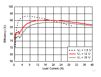
| VOUT = 1 V | SKIP Mode | fSW = 650 kHz |
| VDD = 5 V |
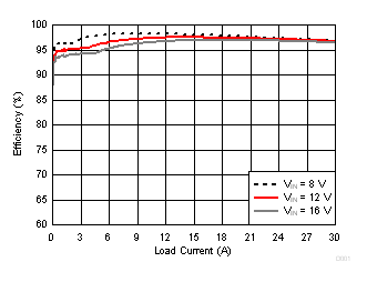
| VOUT = 5.5 V | SKIP Mode | fSW = 425 kHz |
| VDD = 5 V |
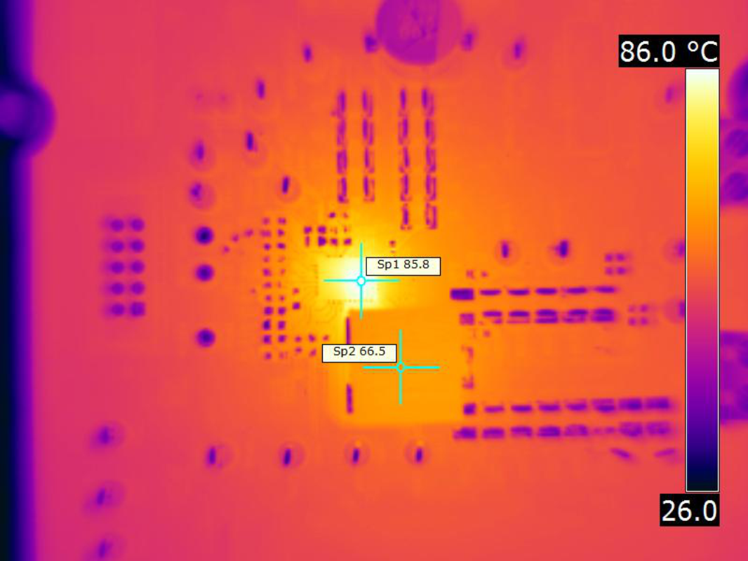
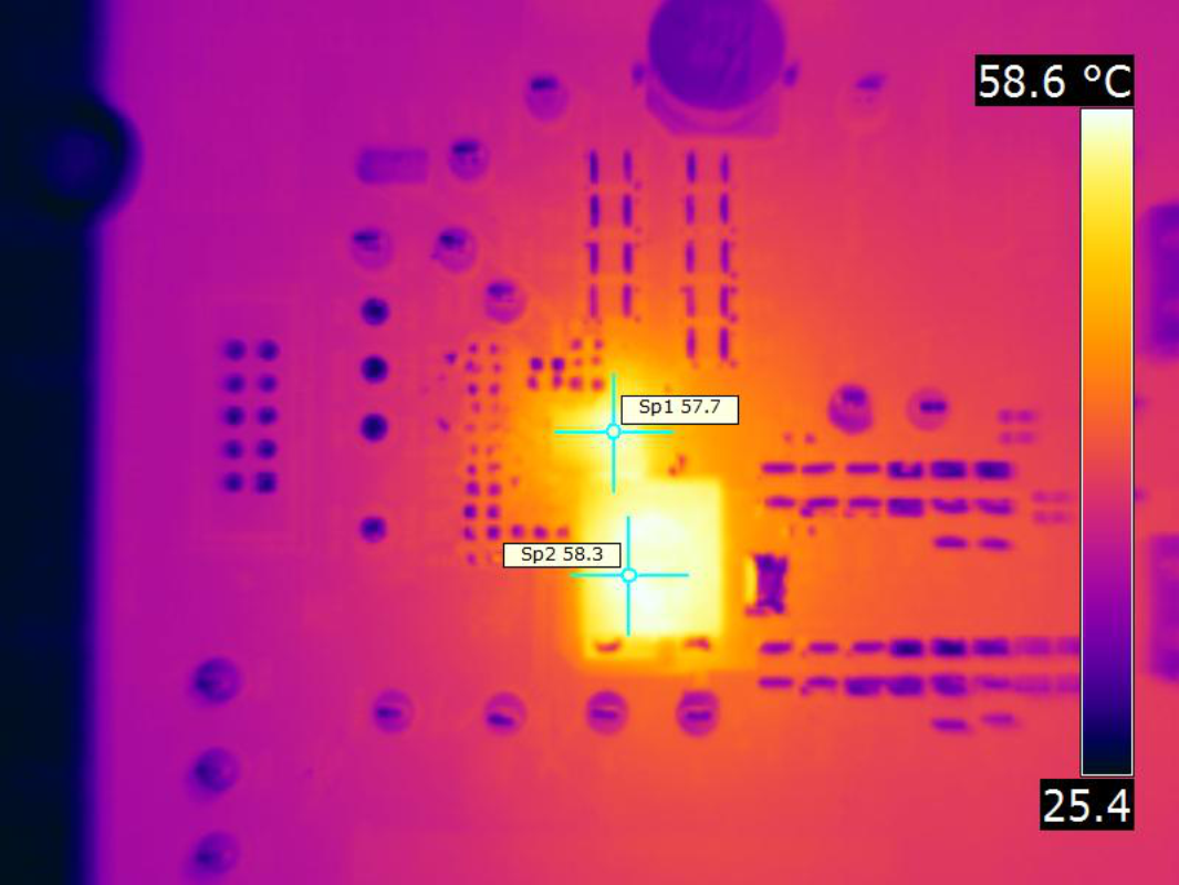
| VIN = 12 V | fSW = 650 kHz | IOUT = 40 A |
| VOUT = 1 V | Natural convection |
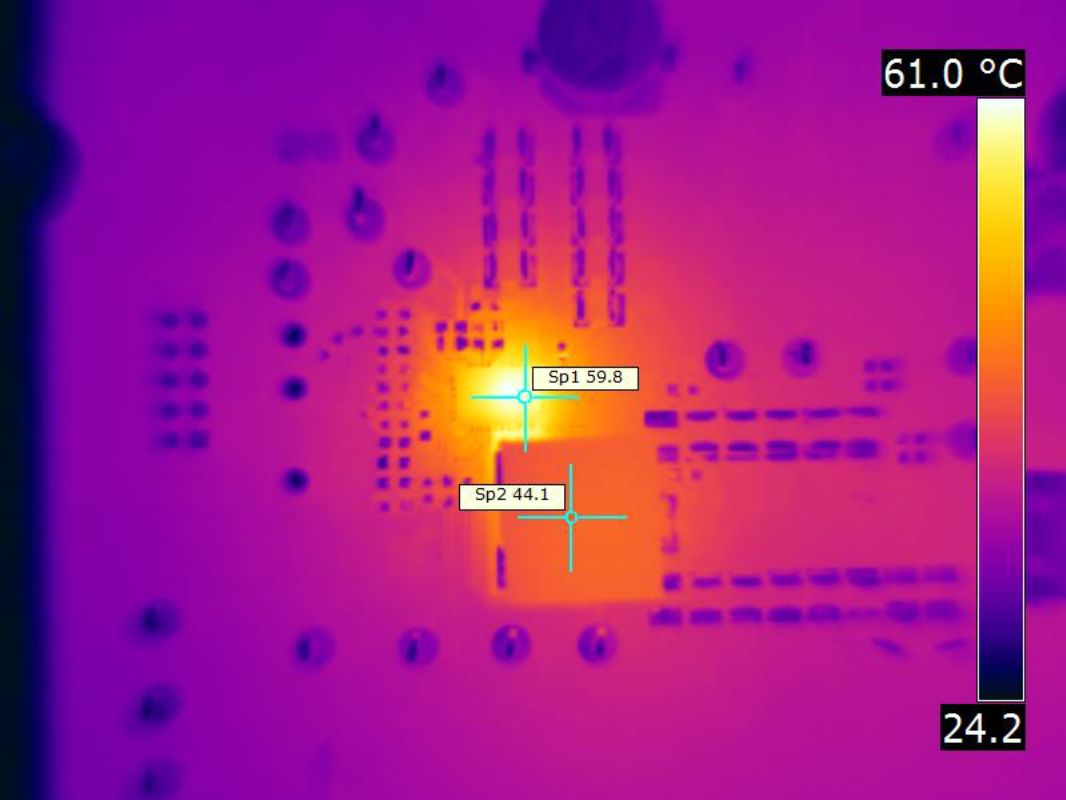
| VIN = 12 V | fSW = 650 kHz | IOUT = 40 A |
| VOUT = 1 V | Airflow = 400 LFM |
| VIN = 12 V | fSW = 425 kHz | IOUT = 30 A |
| VOUT = 5.5 V | Airflow = 200 LFM |
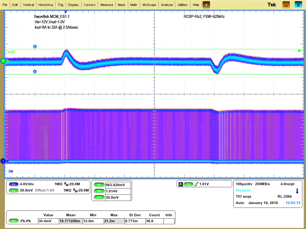
| VOUT = 1 V | VIN = 12 V | |
| IOUT from 8 A to 32 A | 2.5 A/µs |
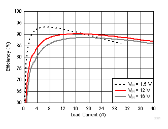
| VOUT = 1 V | FCCM | fSW = 650 kHz |
| VDD = 5 V |
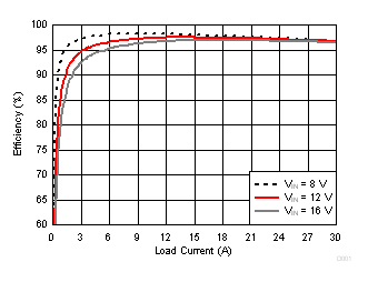
| VOUT = 5.5 V | FCCM | fSW = 425 kHz |
| VDD = 5 V |
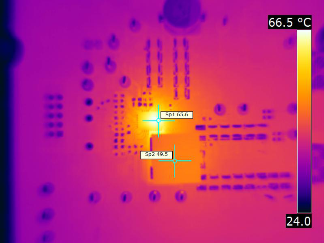
| VIN = 12 V | fSW = 650 kHz | IOUT = 40 A |
| VOUT = 1 V | Airflow = 200 LFM |
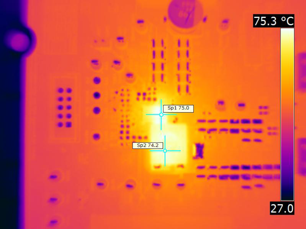
| VIN = 12 V | fSW = 425 kHz | IOUT = 30 A |
| VOUT = 5.5 V | Natural convection |
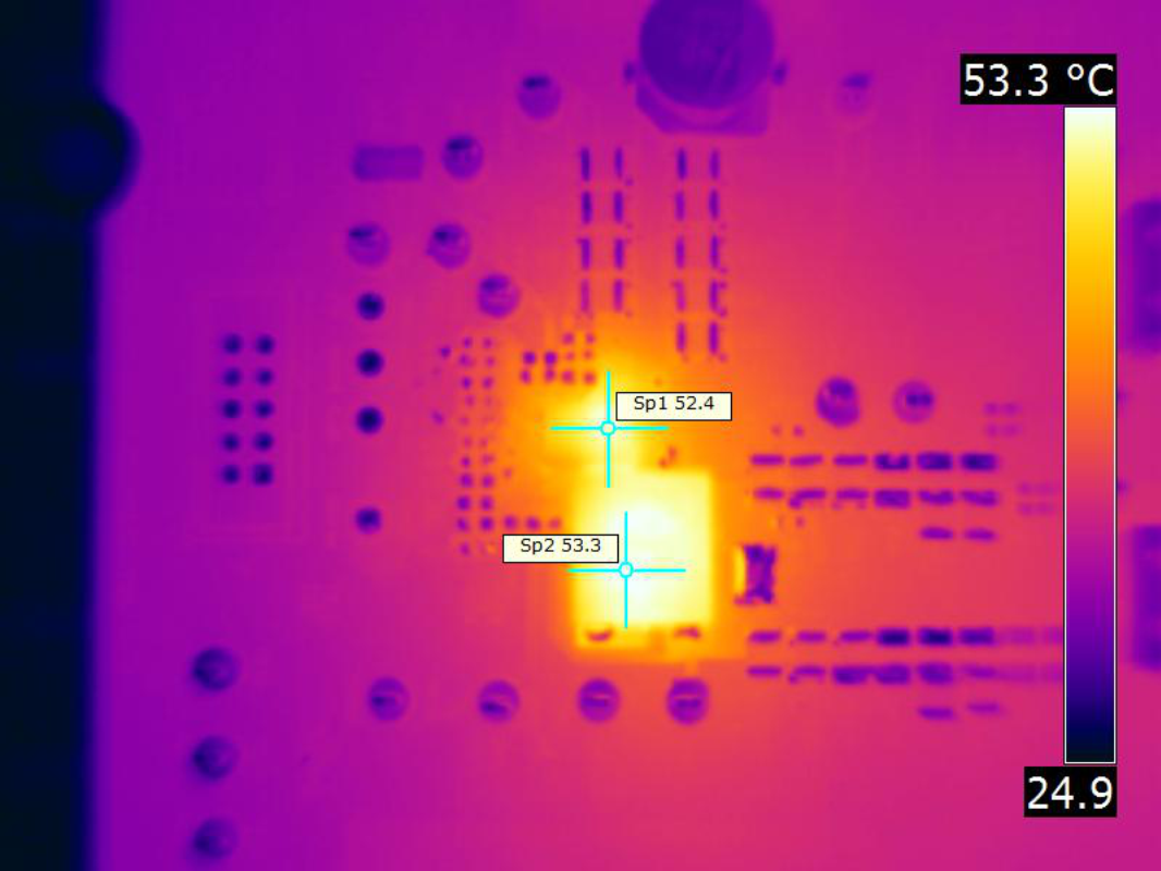
| VIN = 12 V | fSW = 425 kHz | IOUT = 30 A |
| VOUT = 5.5 V | Airflow = 400 LFM |
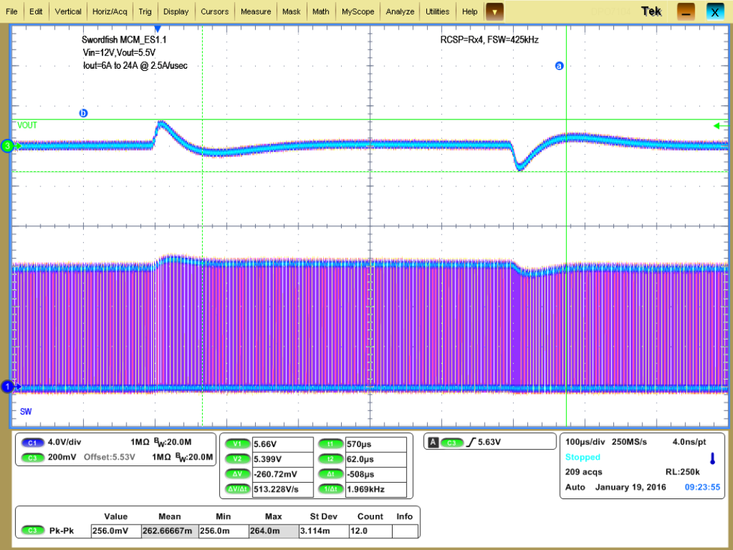
| VOUT = 5.5 V | VIN = 12 V | |
| IOUT from 6 A to 24 A | 2.5 A/µs | |
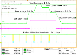
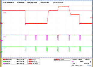
| 1 – Operation only | 4 – Vout Command up to 1.2 V | |||
| 2 – Turn off | 5 – Vout Command down to 0.6 V | |||
| 3 – Turn on without Margin | 6 – Turn off | |||
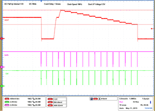
| 1 – Operation only | 4 – 16 Vout Command up to 1.2 V, | |||
| 2 – Turn off | 50 mV per step down to 0.6 V | |||
| 3 – Turn on without Margin | 17 – Turn off | |||
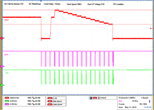
| 1 – Operation only | 4 – 16 Vout Command up to 1.2 V, | |||
| 2 – Turn off | 50 mV per step down to 0.6 V | |||
| 3 – Turn on without Margin | 17 – Turn off | |||
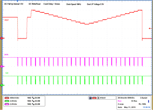
| 1 – Operation only | 4 – 16 Vout Command up to 1.2 V, | |||
| 2 – Turn off | 50 mV per step down to 0.6 V | |||
| 3 – Turn on without Margin | 17 – 28 Vout Command from 0.6 V to 1.2 V, 50 mV per step |
|||
| 29 – Turn off | ||||
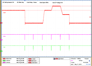
| 1 – Operation only | 4 – Vout Command up to 1.2 V | |||
| 2 – Turn off | 5 – Vout Command down to 0.6 V | |||
| 3 – Turn on without Margin | 6 – Turn off | |||
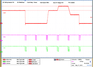
| 1 – Operation only | 4 – Vout Command up to 1.2 V | |||
| 2 – Turn off | 5 – Vout Command down to 0.6 V | |||
| 3 – Turn on without Margin | 6 – Turn off | |||
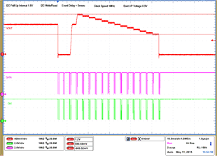
| 1 – Operation only | 4 – 16 Vout Command up to 1.2 V, | |||
| 2 – Turn off | 50 mV per step down to 0.6 V | |||
| 3 – Turn on without Margin | 17 – Turn off | |||
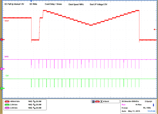
| 1 – Operation only | 4 – 16 Vout Command up to 1.2 V, | |||
| 2 – Turn off | 50 mV per step down to 0.6 V | |||
| 3 – Turn on without Margin | 17 – 28 Vout Command from 0.6 V to 1.2 V, 50 mV per step |
|||
| 29 – Turn off | ||||
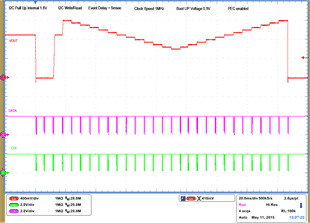
| 1 – Operation only | 4 – 16 Vout Command up to 1.2 V, | |||
| 2 – Turn off | 50 mV per step down to 0.6 V | |||
| 3 – Turn on without Margin | 17 – 28 Vout Command from 0.6 V to 1.2 V, 50 mV per step |
|||
| 29 – Turn off | ||||