JAJSQV6 February 2024 TPS54KC23
PRODUCTION DATA
- 1
- 1 特長
- 2 アプリケーション
- 3 概要
- 4 Pin Configuration and Functions
- 5 Specifications
-
6 Detailed Description
- 6.1 Overview
- 6.2 Functional Block Diagram
- 6.3
Feature Description
- 6.3.1 Internal VCC LDO and Using External Bias On the VCC Pin
- 6.3.2 Enable
- 6.3.3 Adjustable Soft Start
- 6.3.4 Power Good
- 6.3.5 Output Voltage Setting
- 6.3.6 Remote Sense
- 6.3.7 D-CAP4 Control
- 6.3.8 Multifunction Select (MSEL) Pin
- 6.3.9 Low-side MOSFET Zero-Crossing
- 6.3.10 Current Sense and Positive Overcurrent Protection
- 6.3.11 Low-side MOSFET Negative Current Limit
- 6.3.12 Overvoltage and Undervoltage Protection
- 6.3.13 Output Voltage Discharge
- 6.3.14 UVLO Protection
- 6.3.15 Thermal Shutdown
- 6.4 Device Functional Modes
-
7 Application and Implementation
- 7.1 Application Information
- 7.2
Typical Application
- 7.2.1 Design Requirements
- 7.2.2
Detailed Design Procedure
- 7.2.2.1 Output Voltage Setting Point
- 7.2.2.2 Choose the Switching Frequency and the Operation Mode
- 7.2.2.3 Choose the Inductor
- 7.2.2.4 Set the Current Limit (ILIM)
- 7.2.2.5 Choose the Output Capacitor
- 7.2.2.6 RAMP Selection
- 7.2.2.7 Choose the Input Capacitors (CIN)
- 7.2.2.8 Soft-Start Capacitor (SS Pin)
- 7.2.2.9 EN Pin Resistor Divider
- 7.2.2.10 VCC Bypass Capacitor
- 7.2.2.11 BOOT Capacitor
- 7.2.2.12 RC Snubber
- 7.2.2.13 PG Pullup Resistor
- 7.2.3 Application Curves
- 7.3 Power Supply Recommendations
- 7.4 Layout
- 8 Device and Documentation Support
- 9 Revision History
- 10Mechanical, Packaging, and Orderable Information
6.3.7 D-CAP4 Control
The device uses D-CAP4 control to achieve a fast load transient response while maintaining ease-of-use. The D-CAP4 control architecture includes an internal ripple generation network enabling the use of very low-ESR output capacitors such as multi-layered ceramic capacitors (MLCC) and low ESR polymer capacitors. No external current sensing network or voltage compensators are required with D-CAP4 control architecture. The role of the internal ripple generation network is to emulate the ripple component of the inductor current information and then combine with the voltage feedback signal to regulate the loop operation.
D-CAP4 control architecture reduces loop gain variation across VOUT, enabling a fast load transient response across the entire output voltage range with one ramp setting. The R-C time-constant of the internal ramp circuit sets the zero frequency of the ramp, similar to other R-C based internal ramp generation architectures. The reduced variation in loop gain also mitigates the need for a feedforward capacitor to optimize the transient response. The ramp amplitude varies with VIN to minimize variation in loop gain across input voltage, commonly referred to as input voltage feedforward. Lastly, the device uses internal circuitry to correct for the dc offset caused by the injected ramp, and removes the dc offset caused by the output ripple voltage, especially with light load current when skip mode operation is selected.
Table 6-1 gives details on the different ramp settings selectable through the MSEL resistor value shown in Table 6-3. The ramp amplitudes are given relative to RAMP1.
| 1*Ramp | Relative Ramp Amplitude | Zero Location (kHz) |
|---|---|---|
| VREF = 0.5V | ||
| RAMP1 | 1× | 32 |
| RAMP2 | 1.8× | 32 |
| RAMP3 | 1.6× | 53 |
| RAMP4 | 3.0× | 53 |
RAMP2 and RAMP3 result in similar loop bandwidth as the ramp amplitudes are similar. The primary difference between these two settings is the ramp zero frequency. The lower ramp zero location for RAMP2 increases phase margin. However, RAMP3 provides faster transient response than RAMP2 because RAMP3 gives higher gain across the entire frequency range due to smaller ramp amplitude and higher ramp zero location. For most applications, RAMP3 must be used instead of RAMP2. RAMP2 can be used to provide phase boost in applications using an L-C whose double pole frequency allows using RAMP1 but where minimizing jitter is more important than faster transient response. Figure 6-3 and Figure 6-4 show how the loop characteristics changes with the different ramp settings for devices with a 0.5V reference.

| VIN = 12V | fSW = 1100kHz | VOUT = 0.8V |
| Load = 50mΩ | LOUT = 150nH | COUT = 12 × 47µF |

| VIN = 12V | fSW = 1100kHz | VOUT = 0.8V |
| Load = 50mΩ | LOUT = 150nH | COUT = 12 × 47µF |
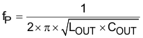
For any control topologies supporting no external compensation, there is a minimum range, maximum range, or both, for the output filter the control topologies can support. The output filter used for a typical buck converter is a low-pass L-C circuit. This L-C filter has double pole that is described in Equation 3.
At low frequencies, the overall loop gain is set by the output set-point resistor divider network and the internal gain of the device. The low frequency L-C double pole has a 180-degree drop in phase. At the output filter frequency, the gain rolls off at a –40dB per decade rate and the phase drops rapidly. The internal ripple generation network introduces a high-frequency zero that reduces the gain roll off from –40dB to –20dB per decade. The zero also increases the phase by 45 degrees at the zero frequency and by 90 degrees at a decade above the zero frequency.
The inductor and capacitor selected for the output filter must be such that the fP double pole of Equation 3 is located no higher than the value given in Table 6-2, then adjusted based on the nominal duty cycle in the application using Equation 4. Equation 4 scales up the fP(TABLE) because, as the duty cycle increases the gain of the D-CAP4 ramp decreases, so the maximum L-C double pole also increases.
| Switching Frequency (kHz) | Maximum L-C Double Pole Frequency (kHz) | ||
|---|---|---|---|
| RAMP1 | RAMP2 and RAMP3 | RAMP4 | |
| 800 | 15.3 | 19.9 | 26.5 |
| 1100 | 21.0 | 27.4 | 36.4 |
| 1400 | 26.8 | 34.9 | 46.4 |
An L-C double pole frequency that violates these guidelines for each ramp setting can be possible, but must be validated in the application with measurements. Choosing very small output capacitance leads to a high frequency L-C double pole which causes the overall loop gain to stay high until the L-C double pole frequency. Given the zero from the internal ripple generation network is a relatively high frequency as well, the loop with very small output capacitance can have too high of a crossover frequency which can cause instability. In general, where reasonable (or smaller) output capacitance is desired, output ripple requirement and load transient requirement can be used to determine the necessary output capacitance for stable operation. The internal zero is selected by the resistor at the MSEL pin, as described earlier.
If MLCCs are used, consider the derating characteristics to determine the effective output capacitance for the design when calculating the L-C double pole frequency. For example, when using an MLCC with specifications of 10µF, X5R and 6.3V, the derating by DC bias and AC bias are 80% and 50%, respectively. The effective derating is the product of these two factors, which in this case is 40% and 4µF. Consult with capacitor manufacturers for specific characteristics of the capacitors to be used in the application.
As a simplified rule, if an output capacitor with an ESR zero that is less than 10× the L-C double pole frequency, TI recommends to ignore when calculating the L-C double pole frequency for stability purposes. The L-C double pole frequency must be recalculated using only the low ESR MLCCs. For more accurate analysis when using mixed type output capacitors, TI recommends simulations or measurements.
For the maximum output capacitance recommendation, select the inductor and capacitor values so that the L-C double pole frequency is no less than 1/100th of the operating frequency. With this starting point, verify the small signal response on the board using the following criteria: The phase margin at the loop crossover is greater than 50 degrees. The actual maximum output capacitance can go higher as long as phase margin is greater than 50 degrees. However, a small signal measurement (Bode plot) must be done to confirm the design.
If requiring an L-C double pole frequency <1/50th the operating frequency, TI recommends using a mixed type output capacitor to achieve the desired effective capacitance. In addition to providing higher density of capacitance, a bulk capacitor with higher ESR also provides phase boost at the L-C double pole frequency. If only low ESR MLCC capacitors are used with an L-C double pole frequency <1/50th the operating frequency, a feedfoward capacitor (CFF) can be added to provide a zero at 10× the L-C double pole frequency. Besides boosting the phase, a CFF feeds more VOUT node information into the FB node through AC coupling. This feedforward during load transient event enables faster response of the control loop to a VOUT deviation. However, this feedforward during steady state operation also feeds more VOUT ripple and noise into FB. High ripple and noise on FB usually leads to more jitter, or even double-pulse behavior. To determine the final CFF value, impacts to loop stability, load transient performance, ripple, and noise on FB must all be considered. TI recommends using frequency analysis equipment to measure the crossover frequency and the stability margin. In most applications, a feedforward capacitor is typically not required because the D-CAP4 architecture provides high loop bandwidth and adding a feedforward capacitor can result in low stability margin.