SLVSCG0 July 2014 TPS57114-EP
PRODUCTION DATA.
- 1 Features
- 2 Applications
- 3 Description
- 4 Simplified Schematic
- 5 Revision History
- 6 Description (continued)
- 7 Pin Configuration and Functions
- 8 Specifications
-
9 Detailed Description
- 9.1 Overview
- 9.2 Functional Block Diagram
- 9.3
Feature Description
- 9.3.1 Fixed-Frequency Pwm Control
- 9.3.2 Slope Compensation and Output Current
- 9.3.3 Bootstrap Voltage (Boot) and Low-Dropout Operation
- 9.3.4 Error Amplifier
- 9.3.5 Voltage Reference
- 9.3.6 Adjusting the Output Voltage
- 9.3.7 Enable Functionality and Adjusting UVLO
- 9.3.8 Slow-Start or Tracking Pin
- 9.3.9 Constant Switching Frequency and Timing Resistor (RT/CLK Pin)
- 9.3.10 Overcurrent Protection
- 9.3.11 Frequency Shift
- 9.3.12 Reverse Overcurrent Protection
- 9.3.13 Synchronize Using the RT/CLK Pin
- 9.3.14 Power Good (PWRGD Pin)
- 9.3.15 Overvoltage Transient Protection (OVTP)
- 9.3.16 Thermal Shutdown
- 9.3.17 Small-Signal Model for Loop Response
- 9.3.18 Simple Small-Signal Model for Peak-Current Mode Control
- 9.3.19 Small-Signal Model for Frequency Compensation
- 9.4 Device Functional Modes
-
10Application and Implementation
- 10.1 Application Information
- 10.2
Typical Application
- 10.2.1 Design Requirements
- 10.2.2
Detailed Design Procedure
- 10.2.2.1 Selecting the Switching Frequency
- 10.2.2.2 Output Inductor Selection
- 10.2.2.3 Output Capacitor
- 10.2.2.4 Input Capacitor
- 10.2.2.5 Slow-Start Capacitor
- 10.2.2.6 Bootstrap Capacitor Selection
- 10.2.2.7 Output-Voltage and Feedback-Resistor Selection
- 10.2.2.8 Compensation
- 10.2.2.9 Power-Dissipation Estimate
- 10.2.3 Application Curves
- 11Power Supply Recommendations
- 12Layout
- 13Device and Documentation Support
- 14Mechanical, Packaging, and Orderable Information
パッケージ・オプション
メカニカル・データ(パッケージ|ピン)
- RTE|16
サーマルパッド・メカニカル・データ
- RTE|16
発注情報
7 Pin Configuration and Functions
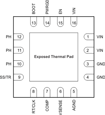
Pin Functions
| PIN | DESCRIPTION | |
|---|---|---|
| NAME | NO. | |
| AGND | 5 | Connect analog ground electrically to GND close to the device. |
| BOOT | 13 | The device requires a bootstrap capacitor between BOOT and PH. Having the voltage on this capacitor below the minimum required by the BOOT UVLO forces the output to switch off until the capacitor recharges. |
| COMP | 7 | Error amplifier output, and input to the output-switch current comparator. Connect frequency-compensation components to this pin. |
| EN | 15 | Enable pin, internal pullup current source. Pull below 1.2 V to disable. Float to enable. An alternative use of this pin can be to set the on-off threshold (adjust UVLO) with two additional resistors. |
| GND | 3 | Power ground. Electrically connect this pin directly to the thermal pad under the IC. |
| 4 | ||
| PH | 10 | The source of the internal high-side power MOSFET and the drain of the internal low-side (synchronous) rectifier MOSFET |
| 11 | ||
| 12 | ||
| PWRGD | 14 | An open-drain output; asserts low if output voltage is low due to thermal shutdown, overcurrent, overvoltage, undervoltage, or EN shutdown. |
| RT/CLK | 8 | Resistor-timing or external-clock input pin. |
| SS/TR | 9 | Slow start and tracking. An external capacitor connected to this pin sets the output-voltage rise time. Another use of this pin is for tracking. |
| VIN | 1 | Input supply voltage, 2.95 to 6 V |
| 2 | ||
| 16 | ||
| VSENSE | 6 | Inverting node of the transconductance (gm) error amplifier |
| Thermal pad | — | Connect the GND pin to the exposed thermal pad for proper operation. Connect this thermal pad to any internal PCB ground plane using multiple vias for good thermal performance. |