SLVSC13A July   2013  – March 2016

PRODUCTION DATA.  

  1. Features
  2. Applications
  3. Description
  4. Revision History
  5. Device Comparison Table
  6. Pin Configuration and Function
  7. Specifications
    1. 7.1 Absolute Maximum Ratings
    2. 7.2 ESD Ratings
    3. 7.3 Recommended Operating Conditions
    4. 7.4 Thermal Information
    5. 7.5 Electrical Characteristics
    6. 7.6 EasyScale Timing Requirements
    7. 7.7 Typical Characteristics
  8. Detailed Description
    1. 8.1 Overview
    2. 8.2 Functional Block Diagram
    3. 8.3 Feature Description
      1. 8.3.1  Normal Operation
      2. 8.3.2  Boost Converter
      3. 8.3.3  IFBx Pin Unused
      4. 8.3.4  Enable and Start-Up
      5. 8.3.5  Soft Start
      6. 8.3.6  Full-Scale Current Program
      7. 8.3.7  Brightness Control
      8. 8.3.8  Undervoltage Lockout
      9. 8.3.9  Overvoltage Protection
      10. 8.3.10 Overcurrent Protection
      11. 8.3.11 Thermal Shutdown
    4. 8.4 Device Functional Modes
      1. 8.4.1 One-Wire Digital Interface (Easyscale Interface)
      2. 8.4.2 PWM Control Interface
    5. 8.5 Programming
      1. 8.5.1 EasyScale Programming
  9. Application and Implementation
    1. 9.1 Application Information
    2. 9.2 Typical Application
      1. 9.2.1 Design Requirements
      2. 9.2.2 Detailed Design Procedure
        1. 9.2.2.1 Inductor Selection
        2. 9.2.2.2 Schottky Diode Selection
        3. 9.2.2.3 Compensation Capacitor Selection
        4. 9.2.2.4 Output Capacitor Selection
      3. 9.2.3 Application Curves
      4. 9.2.4 Additional Application Circuits
  10. 10Power Supply Recommendations
  11. 11Layout
    1. 11.1 Layout Guidelines
    2. 11.2 Layout Example
  12. 12Device and Documentation Support
    1. 12.1 Device Support
      1. 12.1.1 Third-Party Products Disclaimer
    2. 12.2 Community Resources
    3. 12.3 Trademarks
    4. 12.4 Electrostatic Discharge Caution
    5. 12.5 Glossary
  13. 13Mechanical, Packaging, and Orderable Information

パッケージ・オプション

メカニカル・データ(パッケージ|ピン)
サーマルパッド・メカニカル・データ
発注情報

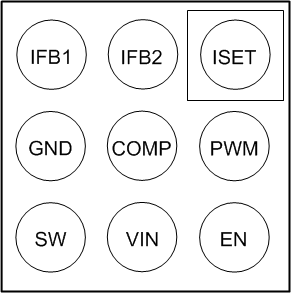
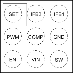
6 Pin Configuration and Function

YFF Package
9-Pin DSBGA
Top View
TPS61162D pin_top_TPS61162D.gif
YFF Package
9-Pin DSBGA
Bottom View
TPS61162D pin_bot_TPS61162D.gif

Pin Functions

PIN I/O DESCRIPTION
NUMBER NAME
A1 ISET I Full-scale LED current set pin. Connecting a resistor to the pin programs the full-scale LED current.
A2 IFB2 I Regulated current sink input pin
A3 IFB1 I Regulated current sink input pin
B1 PWM I PWM dimming signal input
B2 COMP O Output of the transconductance error amplifier. Connect external capacitor to this pin to compensate the boost loop.
B3 GND O Ground
C1 EN I Enable control and one-wire digital signal input
C2 VIN I Supply input pin
C3 SW I Drain connection of the internal power MOSFET