SLVSCN9B December 2014 – June 2020 TPS61175-Q1
PRODUCTION DATA.
- 1 Features
- 2 Applications
- 3 Description
- 4 Revision History
- 5 Pin Configuration and Functions
- 6 Specifications
- 7 Detailed Description
-
8 Application and Implementation
- 8.1 Application Information
- 8.2
Typical Application
- 8.2.1 Design Requirements
- 8.2.2
Detailed Design Procedure
- 8.2.2.1 Determining the Duty Cycle
- 8.2.2.2 Selecting the Inductor
- 8.2.2.3 Computing the Maximum Output Current
- 8.2.2.4 Setting Output Voltage
- 8.2.2.5 Setting the Switching Frequency
- 8.2.2.6 Setting the Soft Start Time
- 8.2.2.7 Selecting the Schottky Diode
- 8.2.2.8 Selecting the Input and Output Capacitors
- 8.2.2.9 Compensating the Small Signal Control Loop
- 8.2.3 Application Curves
- 9 Power Supply Recommendations
- 10Layout
- 11Device and Documentation Support
- 12Mechanical, Packaging, and Orderable Information
パッケージ・オプション
メカニカル・データ(パッケージ|ピン)
- PWP|14
サーマルパッド・メカニカル・データ
- PWP|14
発注情報
6.7 Typical Characteristics
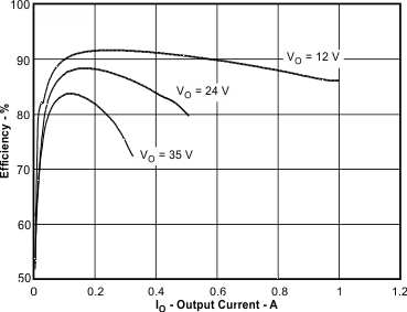
| VI = 5 V |
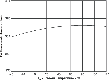 Figure 3. Error Amplifier Transconductance vs Free-Air Temperature
 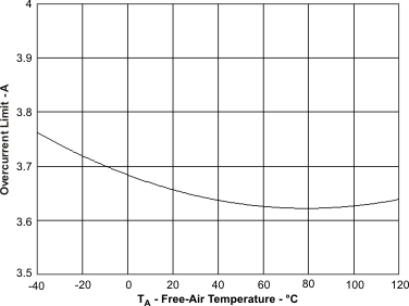 Figure 5. Overcurrent Limit vs Free-Air Temperature
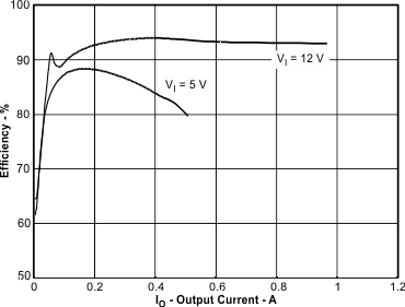
| VO = 24 V |
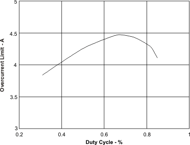 Figure 4. Overcurrent Limit vs Duty Cycle
 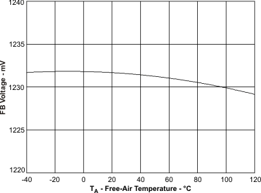 Figure 6. FB Voltages Free-Air Temperature