SLVSCK4A September 2015 – May 2016 TPS61235P , TPS61236P
PRODUCTION DATA.
- 1 Features
- 2 Applications
- 3 Description
- 4 Revision History
- 5 Device Comparison Table
- 6 Pin Configuration and Functions
- 7 Specifications
-
8 Detailed Description
- 8.1 Overview
- 8.2 Functional Block Diagram
- 8.3
Feature Description
- 8.3.1 Boost Controller Operation
- 8.3.2 Soft Start
- 8.3.3 Enable and Disable
- 8.3.4 Constant Output Voltage and Constant Output Current Operations
- 8.3.5 Over Current Protection
- 8.3.6 Load Status Indication
- 8.3.7 Under voltage Lockout
- 8.3.8 Over Voltage Protection and Reverse Current Block
- 8.3.9 Short Circuit Protection
- 8.3.10 Thermal Shutdown
- 8.4 Device Functional Modes
-
9 Applications and Implementation
- 9.1 Application Information
- 9.2
Typical Applications
- 9.2.1
TPS61236P 3-V to 4.35-V Input, 5-V Output Voltage, 3-A Maximum Output Current
- 9.2.1.1 Design Requirements
- 9.2.1.2 Detailed Design Procedure
- 9.2.1.3 TPS61236P 5-V Output Application Curves
- 9.2.2 TPS61236P 2.3-V to 5-V Input, 5-V 2-A Output Converter
- 9.2.1
TPS61236P 3-V to 4.35-V Input, 5-V Output Voltage, 3-A Maximum Output Current
- 10Power Supply Recommendations
- 11Layout
- 12Device and Documentation Support
- 13Mechanical, Packaging, and Orderable Information
9 Applications and Implementation
NOTE
Information in the following applications sections is not part of the TI component specification, and TI does not warrant its accuracy or completeness. TI’s customers are responsible for determining suitability of components for their purposes. Customers should validate and test their design implementation to confirm system functionality.
9.1 Application Information
The TPS6123x family is designed to operate from an input voltage supply range from 2.3-V to (VOUT – 0.6)-V, and the maximum output voltage can be up to 5.5-V. The device operates in PWM mode under medium to heavy load conditions and in power save mode under light load condition. In PWM mode, the TPS6123x converter operates with 1-MHz switching frequency which provides a controlled frequency variation over the input voltage range. As load current decreases, the converter enters PFM mode, reducing switching frequency and minimizing IC quiescent current to achieve high efficiency over the entire load current range. The TPS6123x also supports a constant current output feature to limit the maximum output current at a programmed value.
9.2 Typical Applications
9.2.1 TPS61236P 3-V to 4.35-V Input, 5-V Output Voltage, 3-A Maximum Output Current
This example illustrates how to use the TPS61236P to generate a 5-V output voltage from a Li-ion battery input and how to use the CC function to limit maximum output current to 3-A for the entire input voltage range.
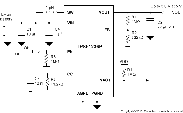 Figure 16. TPS61236P 5-V Output with 3-A Constant Output Current
9.2.1.1 Design Requirements
The design parameters for the TPS61236P 5-V 3-A constant output current design are listed in Table 1.
Table 1. TPS61236P 5-V 3-A Constant Output Current Design Parameters
| DESIGN PARAMETERS | EXAMPLE VALUES |
|---|---|
| Input voltage range | 3 V to 4.35 V |
| Output voltage | 5 V |
| Output current limit | 3 A |
| Operating frequency | 1 MHz |
9.2.1.2 Detailed Design Procedure
The following sections describe the selection process of the external components. The following table summaries the final component selections.
Table 2. List of Components for TPS61236P 5-V Output with 3-A Constant Output Current Application
| REFERENCE | DESCRIPTION | MANUFACTURER(1) |
|---|---|---|
| L1 | 1.0 μH, Power Inductor, XAL7030 | Coilcraft |
| C1 | 10 μF 6.3 V, 0603, X5R ceramic, GRM188R60J106ME84 | Murata |
| C2 | 3 × 22 μF 10 V, 0805, X5R ceramic, GRM21BR61A226ME44 | Murata |
| C3 | 10 nF, 50 V, 0603, X5R ceramic, GRM188R61H103KA01D | Murata |
| C4 | 1 µF, 6.3 V, 0402, X5R ceramic, GRM152R60J105ME15 | Murata |
| R1 | 1 MΩ, Resistor, Chip, 1/10W, 1% | Rohm |
| R2 | 332 kΩ, Resistor, Chip, 1/10W, 0.5% | Rohm |
| R3 | 41.2 kΩ, Resistor, Chip, 1/10W, 0.5% | Rohm |
| R4 | 1 MΩ, Resistor, Chip, 1/10W, 1% | Rohm |
| R5 | 1 MΩ, Resistor, Chip, 1/10W, 1% | Rohm |
9.2.1.2.1 Programming the Output Voltage
The TPS61236P's output voltage needs to be programmed via an external voltage divider at the FB pin, as shown in Figure 16.
By selecting R1 and R2, the output voltage is programmed to the desired value. When the output voltage is regulated, the typical voltage at the FB pin is VFB. The following equation can be used to calculate R1 and R2.

For the best accuracy, the current following through R2 should be 100 times larger than FB pin leakage current. Changing R2 towards a lower value increases the robustness against noise injection. Changing R2 towards higher values reduces the FB divider current for achieving the highest efficiency at low load currents.
For the fixed output voltage version, TPS61235P, the FB pin must be tied to the output directly.
In this example, 1-MΩ and 332-kΩ resistors are selected for R1 and R2. High accuracy like 0.5% resistors are recommended for better output voltage accuracy.
9.2.1.2.2 Program the Constant Output Current
The TPS6123x's constant output current can be programmed via an external resistor RCC at the CC pin.
Because the TPS6123x has an internal current limit function to protect the IC from over load situations, a user should make sure the constant output current is set within the device's maximum load capability. If the constant current is set too high, the output current will be limited by internal protection circuitry and cannot reach the set value.
The maximum output capability is determined by the input to output voltage ratio and the internal current limit ILIM. Refer to Equation 3, Equation 4, and Equation 5 for the maximum output current calculation. The minimum input voltage, minimum current limit value, and maximum switching frequency value shall be used for the worst case calculation.
In this example, the minimum input voltage is 3-V and output voltage is 5-V. The efficiency η can be estimated as 85% for the worst case condition. By checking the specification table, the minimum ILIM value is 6.5-A, and maximum switching frequency fSW is 1250-kHz, so the calculation result of the maximum output current under the worse case condition is 3.6-A.
After calculation, the 3-A constant current target is within the maximum output current range, so the user can set it. Equation 2 can be used to select RCC (R3 in Figure 16). In this example, the calculation result of R3 is 41.47-kΩ. A 1% accuracy 41.2-kΩ resistor is selected. By using it, the constant output current can be regulated at 3-A typically.
C3 must be connected in parallel with R3 to average the CC pin voltage and also stabilize the control loop. A larger capacitor can smooth the CC voltage better, and also slow down the loop response. Normally a 10-nF capacitor is recommended.
If the Constant Current function is not needed, the user can simply connect the CC pin to ground to disable it. Under this configuration, the TPS6123x works as a normal boost converter, and its maximum output current is decided by the internal current limit circuitry.
9.2.1.2.3 Inductor and Capacitor Selection
A boost converter requires two main passive components for storing energy during the conversion, an inductor and an output capacitor. Please refer to the following sections to select the inductor and capacitor. Also refer to the Recommended Operating Conditions for operation recommendations.
9.2.1.2.3.1 Inductor Selection
Because a 1-µH inductor normally has a higher current rating and smaller form factor than inductors of higher values, the TPS6123x is optimized for 1-µH inductor operation. Inductors of other values may cause control loop instability and so are not recommended.
It is advisable to select an inductor with a saturation current ISAT higher than the possible peak current flowing through the inductor. The inductor's current rating IRMS should be higher than the average input current. The inductor peak current varies as a function of the load, the input and output voltages, and can be estimated by using Equation 7.

Where:
D is the duty cycle, and can be calculated by using Equation 5.
When estimating inductor peak current and average input current, the minimum input voltage, maximum output current, and minimum switching frequency in the application should be used for the worst case calculation. In this example, the minimum VIN is 3.0-V, maximum IOUT is 3-A, and minimum fsw is 750-kHz, so the inductor peak current result is 6.9-A, and the average input current is 5.9-A with an 85% efficiency estimation.
Selecting an inductor with insufficient saturation current can lead to excessive peak current in the converter. This could eventually harm the device and reduce reliability. To leave enough margin, it is recommended to choose saturation current 20% to 30% higher than IL_PEAK.
The following inductors are recommended to be used in designs if the current rating allows.
Table 3. List of Inductors
| INDUCTANCE [µH] | ISAT [A] | IRMS [A] | DC RESISTANCE [mΩ] | PART NUMBER | MANUFACTURER(1) |
|---|---|---|---|---|---|
| 1 | 28 | 21.8 | 4.55 | XAL7030-102ME | Coilcraft |
| 1 | 14.1 | 13 | 7.1 | SPM6530T-1R0M120 | TDK |
| 1 | 19 | 11 | 9 | FDSD0630-H-1R0M | TOKO |
| 1 | 11 | 6 | 23 | SPM5020T-1R0M | TDK |
9.2.1.2.3.2 Output Capacitor Selection
For the output capacitor, it is recommended to use small X5R or X7R ceramic capacitors placed as close as possible to the VOUT and PGND pins of the IC. If, for any reason, the application requires the use of large capacitors which cannot be placed close to the IC, using a smaller ceramic capacitor of 1-µF or 0.1-µF in parallel to the large one is highly recommended. This small capacitor should be placed as close as possible to the VOUT and PGND pins of the IC.
The TPS6123x requires at least 20-µF effective capacitance at output for stability consideration. Care must be taken when evaluating a capacitor’s derating under bias. The bias can significantly reduce the effective capacitance. Ceramic capacitors can have losses of as much as 50% of their capacitance at rated voltage. Therefore, leave margin on the voltage rating to ensure adequate effective capacitance. In this example, three 22-µF capacitors of 10-V rating are used.
The ESR impact on the output ripple must be considered as well if tantalum or electrolytic capacitors are used. Assuming there is enough capacitance such that the ripple due to the capacitance can be ignored, the ESR needed to limit the VRipple is:

9.2.1.2.3.3 Input Capacitor Selection
Multilayer X5R or X7R ceramic capacitors are an excellent choice for input decoupling of the step-up converter as they have extremely low ESR and are available in small footprints. Input capacitors should be located as close as possible to the device. The required minimum effective capacitance at input for the TPS6123x is 4.7-µF. Considering the capacitor’s derating under bias, a 10-µF input capacitor is recommended, and a 22-μF input capacitor should be sufficient for most applications. There is no limitation to use larger capacitors. It is recommended to put the input capacitor close to the VIN and PGND pins of the IC. If, for any reason, the input capacitor cannot be placed close to the IC, putting a small ceramic capacitor of 1-µF or 0.1-µF close to the IC's VIN pin and ground pin is recommended.
Take care when a ceramic capacitor is used at the input and the power is being supplied through long wires, such as from a wall adapter. A load step at the output may cause ringing at the VIN pin due to the inductance of the long wires. This ringing can couple to the output and be mistaken as loop instability or could even damage the part. Additional bulk capacitance (electrolytic or tantalum) should in this circumstance be placed between CIN and the power source to reduce ringing.
9.2.1.2.4 Loop Stability, Feed Forward Capacitor
One approach of stability evaluation is to look from a steady-state perspective at the following signals:
- Switching node, SW
- Inductor current, IL
- Output ripple, VRipple(OUT)
When the switching waveform shows large duty cycle jitter or the output voltage or inductor current shows oscillations, the regulation loop may be unstable. This is often a result of board layout and/or L-C combination.
Load transient response is another approach to check loop stability. During the load transient recovery time, VOUT can be monitored for settling time, overshoot, or ringing that helps judge the converter’s stability. Without any ringing, the loop has usually more than 45° of phase margin.
To improve output voltage undershoot and overshoot performance during heavy load transient such as a 2-A load step transient, a feed forward capacitor Cff in parallel with R1 is recommended, as shown in Figure 17. The feed forward capacitor increases the loop bandwidth by adding a zero, so to achieve smaller output voltage undershoot, as shown in Figure 25. A 10-pF capacitor is suitable for most applications of the TPS6123x. See Application Note SLVA289 for more application notes of feed forward capacitor.
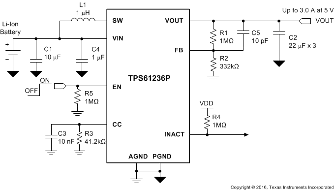 Figure 17. TPS61236P with Cff
9.2.1.2.5 INACT Pin Pull-up Resistor
The INACT pin can be used to report boost converter loading status to the MCU. It is an open drain output and should be connected with a pull up resistor. Normally a 1-MΩ resistor is recommended for the pull up resistor.
9.2.1.3 TPS61236P 5-V Output Application Curves
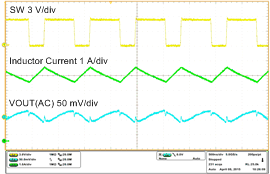
| VIN = 3.6 V, VOUT = 5 V, IOUT = 3.1 A | ||
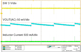
| VIN = 3.6 V, VOUT = 5 V, IOUT = 0 mA | ||
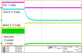
| VIN = 3.6 V, VOUT = 5 V, RL = 2.5 Ω | ||
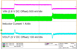
| VIN = 2.8 V to 3.3 V, VOUT = 5 V, IOUT = 2 A | ||
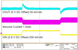
| VIN = 2.8 V to 3.3 V, VOUT = 5 V, IOUT = 2 A, Cff = 10 pF | ||
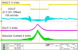
| VIN = 3.6 V, VOUT = 5 V, CC = 3.0 A, IOUT from 0 mA to 3 A | ||
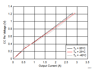
| RCC = 41.2 kΩ (CC current set to 3 A), VIN = 3.6 V | ||
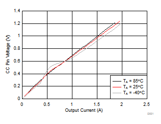
| RCC = 61.9 kΩ (CC current set to 2 A), VIN = 3.6 V |
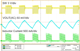
| VIN = 3.6 V, VOUT = 5 V, IOUT = 100 mA | ||
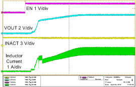
| VIN = 3.6 V, VOUT = 5 V, RL = 2.5 Ω | ||
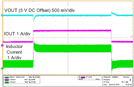
| VIN = 3.6 V, VOUT = 5 V, IOUT = 500 mA to 2 A | ||
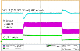
| VIN = 3.6 V, VOUT = 5 V, IOUT = 500 mA to 2 A, Cff = 10 pF | ||
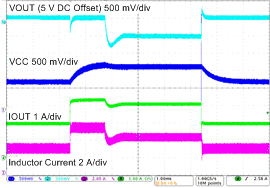
| VIN = 3.6 V, VOUT = 5.1 V, RCC = 41.2 kΩ, RL = 2.5 Ω to 1.5 Ω | ||
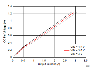
| RCC = 41.2 kΩ (CC current set to 3 A), TA = 25°C | ||
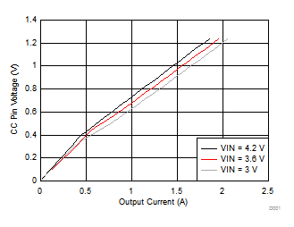
| RCC = 61.9 kΩ (CC current set to 2 A), TA = 25°C | ||
9.2.2 TPS61236P 2.3-V to 5-V Input, 5-V 2-A Output Converter
In this application, the TPS6123x is required to be used as a standard boost converter to output 5-V voltage and maximum 2-A current. The Constant Current function should be disabled, and the INACT function is not needed either.
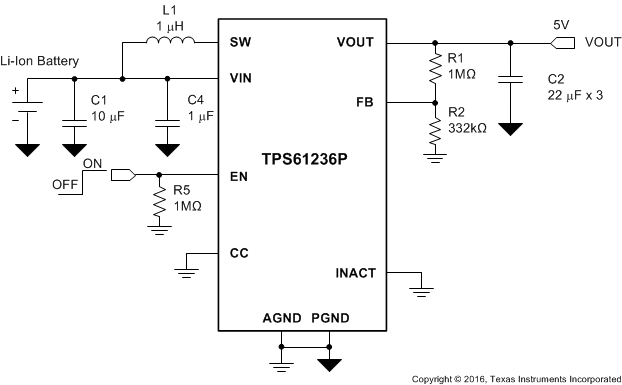 Figure 33. TPS61236P 5-V 2-A Output Typical Application
9.2.2.1 Design Requirements
The design parameters for the TPS61236P 5-V output current design are listed in Table 4.
Table 4. TPS61236P 5-V Output Design Parameters
| DESIGN PARAMETERS | EXAMPLE VALUES |
|---|---|
| Input voltage range | 2.3 V to 4.4 V |
| Output voltage | 5 V |
| Output current rating | 2 A |
| Operating frequency | 1 MHz |
9.2.2.2 Detailed Design Procedure
Refer to the Detailed Design Procedure section for the detailed design steps.
Because the CC function and the INACT function are not needed, the user can simply connect the two pins to ground to disable the functions as shown in Figure 33.
9.2.2.3 TPS61236P 5-V Output Application Curves
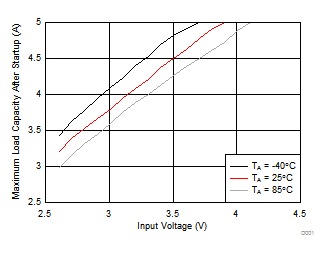
| VOUT = 5.1 V (TPS61235P), CC pin connected to GND | ||
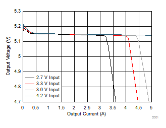
| VOUT = 5.1 V (TPS61235P), CC pin connected to GND | ||
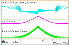
| VIN = 3.6 V, VOUT = 5 V, IOUT from 0 mA to 4 A | ||
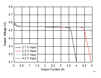
| VOUT = 4.5 V (TPS61236P), CC pin connected to GND | ||
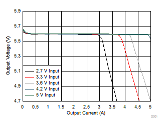
| VOUT = 5.5 V (TPS61236P), CC pin connected to GND | ||