JAJSFB0E January 2018 – February 2024 TPS61322
PRODUCTION DATA
- 1
- 1 特長
- 2 アプリケーション
- 3 概要
- 4 Device Comparison Table
- 5 Pin Configuration and Functions
- 6 Specifications
- 7 Detailed Description
- 8 Application and Implementation
- 9 Power Supply Recommendations
- 10Layout
- 11Device and Documentation Support
- 12Revision History
- 13Mechanical, Packaging, and Orderable Information
パッケージ・オプション
メカニカル・データ(パッケージ|ピン)
サーマルパッド・メカニカル・データ
発注情報
8.2.1.2.2 Maximum Output Current
For boost converters, the maximum output current capability is determined by the input to output ratio, the efficiency, the inductor current ripple and the current limit. The maximum output current can be estimated by Equation 1
Equation 1. 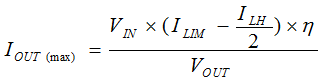
where
- ILIM is the peak inductor current limit
- ILH is the inductor current ripple
- η is the boost converter power convert efficiency
Minimum input voltage, maximum boost output voltage and minimum current limit should be used as the worst case condition for the estimation.
In this example, assume the power efficiency is 70% at the minimum input voltage of 0.9 V. The calculated maximum output current is 114 mA, which satisfies the application requirements.