SLVS977B February 2010 – July 2016 TPS61325
PRODUCTION DATA.
- 1 Features
- 2 Applications
- 3 Description
- 4 Revision History
- 5 Device Comparison Table
- 6 Pin Configuration and Functions
- 7 Specifications
- 8 Parameter Measurement Information
-
9 Detailed Description
- 9.1 Overview
- 9.2 Functional Block Diagram
- 9.3
Feature Description
- 9.3.1 LED High-current Regulators, Unused Inputs
- 9.3.2 Safety Timer Accuracy
- 9.3.3 Current Limit Operation
- 9.3.4 Start-Up Sequence
- 9.3.5 Power Good (Flash Ready)
- 9.3.6 LED Temperature Monitoring
- 9.3.7 Hot Die Detector
- 9.3.8 Undervoltage Lockout
- 9.3.9 Storage Capacitor Active Cell Balancing
- 9.3.10 RED Light Privacy Indicator
- 9.3.11 White LED Privacy Indicator
- 9.3.12 Storage Capacitor, Precharge Voltage Calibration
- 9.3.13 Storage Capacitor, Adaptive Precharge Voltage
- 9.3.14 Serial Interface Description
- 9.4
Device Functional Modes
- 9.4.1 Down Mode In Voltage Regulation Mode
- 9.4.2 Power-Save Mode Operation, Efficiency
- 9.4.3 Mode Of Operation: DC-Light and Flashlight
- 9.4.4 Flash Strobe Is Level Sensitive (STT = 0): LED Strobe Follows STRB0 and STRB1 Inputs
- 9.4.5 Flash Strobe Is Leading Edge Sensitive (STT = 1): One-Shot LED Strobe
- 9.4.6 LED Failure Modes and Overvoltage Protection
- 9.4.7 Hardware Voltage Mode Selection
- 9.4.8 Flashlight Blanking (Tx-MASK)
- 9.4.9 Shutdown
- 9.4.10 Thermal Shutdown
- 9.5 Programming
- 9.6
Register Maps
- 9.6.1 Slave Address Byte
- 9.6.2 Register Address Byte
- 9.6.3 REGISTER0 (address = 0x00)
- 9.6.4 REGISTER1 (address = 0x01)
- 9.6.5 REGISTER2 (address = 0x02)
- 9.6.6 REGISTER3 (address = 0x03)
- 9.6.7 REGISTER4 (address = 0x04)
- 9.6.8 REGISTER5 (address = 0x05)
- 9.6.9 REGISTER6 (address = 0x06)
- 9.6.10 REGISTER7 (address = 0x07)
- 10Application and Implementation
- 11Power Supply Recommendations
- 12Layout
- 13Device and Documentation Support
- 14Mechanical, Packaging, and Orderable Information
7 Specifications
7.1 Absolute Maximum Ratings
over operating free-air temperature range (unless otherwise noted)(1)| MIN | MAX | UNIT | ||
|---|---|---|---|---|
| Voltage(2) | AVIN, VOUT, SW, LED1, LED2, LED3, SCL, SDA, STRB0, STRB1, GPIO/PG, HC_SEL, Tx-MASK, TS, and BAL pins | –0.3 | 7 | V |
| Current | GPIO/PG pin | ±25 | mA | |
| Power dissipation | Internally limited | |||
| Operating ambient temperature(3), TA | –40 | 85 | °C | |
| Maximum operating junction temperature, TJ(MAX) | 150 | °C | ||
| Storage temperature, Tstg | –65 | 150 | °C | |
(1) Stresses beyond those listed under Absolute Maximum Ratings may cause permanent damage to the device. These are stress ratings only, which do not imply functional operation of the device at these or any other conditions beyond those indicated under Recommended Operating Conditions. Exposure to absolute-maximum-rated conditions for extended periods may affect device reliability.
(2) All voltage values are with respect to network ground terminal.
(3) In applications where high power dissipation and/or poor package thermal resistance is present, the maximum ambient temperature may have to be derated. Maximum ambient temperature (TA(max)) is dependent on the maximum operating junction temperature (TJ(max)), the maximum power dissipation of the device in the application (PD(max)), and the junction-to-ambient thermal resistance of the part/package in the application (RθJA), as given by the following equation: TA(max) = TJ(max) - ( RθJA × PD(max) )
7.2 ESD Ratings
| VALUE | UNIT | |||
|---|---|---|---|---|
| V(ESD) | Electrostatic discharge | Human-body model (HBM), per ANSI/ESDA/JEDEC JS-001(1) | ±2000 | V |
| Charged-device model (CDM), per JEDEC specification JESD22-C101(2) | ±500 | |||
(1) JEDEC document JEP155 states that 500-V HBM allows safe manufacturing with a standard ESD control process.
(2) JEDEC document JEP157 states that 250-V CDM allows safe manufacturing with a standard ESD control process.
7.3 Recommended Operating Conditions
over operating free-air temperature range (unless otherwise noted)| MIN | NOM | MAX | UNIT | |||
|---|---|---|---|---|---|---|
| VIN | Input voltage | 2.5 | 3.6 | 5.5 | V | |
| VOUT | Output voltage | Current regulation mode | VIN | 5.5 | V | |
| Voltage regulation mode | 3.825 | 5.7 | ||||
| L | Inductor | 1.3 | 2.2 | 2.9 | µH | |
| CIN | Input capacitor | 10 | µF | |||
| COUT | Output capacitor (effective value) | 3 | 10 | µF | ||
7.4 Thermal Information
| THERMAL METRIC(1) | TPS61325 | UNIT | |
|---|---|---|---|
| YFF (DSBGA) | |||
| 20 PINS | |||
| RθJA | Junction-to-ambient thermal resistance | 75.9 | °C/W |
| RθJC(top) | Junction-to-case (top) thermal resistance | 0.4 | °C/W |
| RθJB | Junction-to-board thermal resistance | 13.3 | °C/W |
| ψJT | Junction-to-top characterization parameter | 2 | °C/W |
| ψJB | Junction-to-board characterization parameter | 13.3 | °C/W |
| RθJC(bot) | Junction-to-case (bottom) thermal resistance | — | °C/W |
(1) For more information about traditional and new thermal metrics, see the Semiconductor and IC Package Thermal Metrics application report.
7.5 Electrical Characteristics
Unless otherwise noted the specification applies for VIN = 3.6 V over an operating junction temp. –40°C ≤ TJ ≤ 125°C;Circuit in Parameter Measurement Information (unless otherwise noted). Typical values are for TJ = 25°C.
| PARAMETER | TEST CONDITIONS | MIN | TYP | MAX | UNIT | ||
|---|---|---|---|---|---|---|---|
| SUPPLY CURRENT | |||||||
| VIN | Input voltage range | 2.5 | 5.5 | V | |||
| IQ | Operating quiescent current into AVIN | IOUT = 0 mA, device not switching, –40°C ≤ TJ ≤ 85°C | 590 | 700 | µA | ||
| IOUT(DC) = 0 mA, PWM operation VOUT = 4.95 V, voltage regulation mode |
11.3 | mA | |||||
| ISD | Shutdown current | HC_SEL = 0, –40°C ≤ TJ ≤ 85°C | 1 | 5 | µA | ||
| ISTBY | Standby current | HC_SEL = 1, storage capacitor balanced –40°C ≤ TJ ≤ 85°C |
2 | 12 | µA | ||
| Precharge current | 0 V ≤ VOUT ≤ 3.3 V, device in precharge mode, –40°C ≤ TJ ≤ 85°C |
80 | 180 | 220 | mA | ||
| Precharge termination threshold | VOUT rising, –40°C ≤ TJ ≤ 85°C | 3.35 | 3.6 | V | |||
| Precharge hysteresis (referred to VOUT) | 40 | 75 | mV | ||||
| VUVLO | Undervoltage lockout threshold (analog circuitry) |
VIN falling | 2.3 | 2.4 | V | ||
| OUTPUT | |||||||
| VOUT | Output voltage range | Current regulation mode | VIN | 5.5 | V | ||
| Voltage regulation mode | 3.825 | 5.7 | |||||
| Internal feedback voltage accuracy | 2.5 V ≤ VIN ≤ 4.8 V, –20°C ≤ TJ ≤ 125°C Boost mode, PWM voltage regulation |
–2% | 2% | ||||
| Power-save mode ripple voltage | IOUT = 10 mA | 0.015 VOUT | VP-P | ||||
| OVP | Output overvoltage protection | VOUT rising, 0000 ≤ OV ≤ 0100 | 4.5 | 4.65 | 4.8 | V | |
| VOUT rising, 0101 ≤ OV ≤ 1111 | 5.8 | 6 | 6.2 | ||||
| Output overvoltage protection hysteresis | VOUT falling, 0101 ≤ OV ≤ 1111 | 0.15 | V | ||||
| POWER SWITCH | |||||||
| rDS(on) | Switch MOSFET on-resistance | VOUT = VGS = 3.6 V | 90 | mΩ | |||
| Rectifier MOSFET on-resistance | VOUT = VGS = 3.6 V | 135 | mΩ | ||||
| Ilkg(SW) | Leakage into SW | VOUT = 0 V, SW = 3.6 V, –40°C ≤ TJ ≤ 85°C | 0.3 | 4 | µA | ||
| Ilim | Rectifier valley current limit (open‑loop) | VOUT = 4.95 V, HC_SEL = 0, –20°C ≤ TJ ≤ 85°C, PWM operation, ILIM bit = 0 |
775 | 1150 | 1600 | mA | |
| VOUT = 4.95 V, HC_SEL = 0, –20°C ≤ TJ ≤ 85°C, PWM operation, ILIM bit = 1 |
1050 | 1600 | 2225 | ||||
| VOUT = 4.95 V, HC_SEL = 1, Tx-MASK = 0, –20°C ≤ TJ ≤ 85°C, PWM operation, ILIM bit = 0 |
–85 | 30 | 150 | ||||
| VOUT = 4.95 V, HC_SEL = 1, Tx-MASK = 0, –20°C ≤ TJ ≤ 85°C, PWM operation, ILIM bit = 1 |
175 | 250 | 300 | ||||
| OSCILLATOR | |||||||
| fOSC | Oscillator frequency | 1.92 | MHz | ||||
| fACC | Oscillator frequency | –10% | 7% | ||||
| THERMAL SHUTDOWN, HOT DIE DETECTOR | |||||||
| Thermal shutdown | 140 | 160 | °C | ||||
| Thermal shutdown hysteresis | 20 | °C | |||||
| Hot die detector accuracy | –8 | 8 | °C | ||||
| LED CURRENT REGULATOR | |||||||
| LED1 and LED3 current accuracy | HC_SEL = 0 | 0.4 V ≤ VLED1/3 ≤ 2 V, 0 mA < ILED1/3 ≤ 111 mA, TJ = 85°C |
–10% | 10% | |||
| 0.4 V ≤ VLED2 ≤ 2 V, ILED1/3 > 111 mA, TJ = 85°C | –7.5% | 7.5% | |||||
| LED2 current accuracy | 0.4 V ≤ VLED2 ≤ 2 V, 0 mA < ILED2 ≤ 250 mA, TJ = 85°C |
–10% | 10% | ||||
| 0.4 V ≤ VLED2 ≤ 2 V, ILED2 > 250 mA, TJ = 85°C | –7.5% | 7.5% | |||||
| LED1 and LED3 current accuracy | HC_SEL = 1 | 0.4 V ≤ VLED1/3 ≤ 2 V, 0 mA < ILED1/3 ≤ 1027 mA, TJ = 85°C |
–10% | 10% | |||
| LED2 current accuracy | 0.4 V ≤ VLED2 ≤ 2 V, 0 mA < ILED2 ≤ 2052 mA, TJ = 85°C |
–10% | 10% | ||||
| LED1 and LED3 current matching | HC_SEL = 0 | VLED1/3 = 1 V, ILED1/3 = 444 mA, TJ = 85°C | –7.5% | 7.5% | |||
| LEDx current temperature coefficient | 0.05 | %/°C | |||||
| INDLED current accuracy | 1.5 V ≤ (VIN – VINDLED) ≤ 2.5 V, 0000 ≤ INDC ≤ 0111, TJ = 25°C |
–20% | 20% | ||||
| INDLED current temperature coefficient | 0.04 | %/°C | |||||
| VDO | LEDx sense voltage | ILEDx = full-scale current, HC_SEL = 0 | 400 | mV | |||
| LEDx sense voltage | ILED1/3 = full-scale current, HC_SEL = 1 | 400 | 450 | ||||
| VOUT dropout voltage | IOUT = –15.8 mA, TJ = 25°C, device not switching | 250 | |||||
| LEDx input leakage current | VLEDx = VOUT = 5 V, –40°C ≤ TJ ≤ 85°C | 0.1 | 4 | µA | |||
| INDLED input leakage current | VINDLED = 0 V, –40°C ≤ TJ ≤ 85°C | 0.1 | 1 | µA | |||
| STORAGE CAPACITOR ACTIVE CELL BALANCING | |||||||
| Active cell balancing circuitry quiescent current into VOUT | HC_SEL = 1, storage capacitor balanced –40°C ≤ TJ ≤ 85°C |
1.7 | 3 | µA | |||
| Active cell balancing accuracy | (VOUT – VBAL) vs BAL voltage difference, Storage capacitor balanced HC_SEL = 1, VOUT = 5.7 V |
–100 | 100 | mV | |||
| BAL output drive capability | VOUT = 4.95 V, Sink and source current | ±10 | ±15 | mA | |||
| Active discharge resistor | HC_SEL = 0, device in shutdown mode VOUT to BAL and BAL to GND |
0.85 | 1.5 | kΩ | |||
| LED TEMPERATURE MONITORING | |||||||
| IO(TS) | Temperature sense current source | Thermistor bias current | 23.8 | µA | |||
| TS resistance (warning temperature) | LEDWARN bit = 1, TJ ≥ 25°C | 39 | 44.5 | 50 | kΩ | ||
| TS resistance (hot temperature) | LEDHOT bit = 1, TJ ≥ 25°C | 12.5 | 14.5 | 16.5 | kΩ | ||
| SDA, SCL, GPIO/PG, Tx-MASK, STRB0, STRB1, HC_SEL | |||||||
| V(IH) | High-level input voltage | 1.2 | V | ||||
| V(IL) | Low-level input voltage | 0.4 | V | ||||
| V(OL) | Low-level output voltage (SDA) | IOL = 8 mA | 0.3 | V | |||
| Low-level output voltage (GPIO) | DIR = 1, IOL = 5 mA | 0.3 | |||||
| V(OH) | High-level output voltage (GPIO) | DIR = 1, GPIOTYPE = 0, IOH = 8 mA | VIN - 0.4 | V | |||
| I(LKG) | Logic input leakage current | Input connected to VIN or GND, –40°C ≤ TJ ≤ 85°C | 0.01 | 0.1 | µA | ||
| RPD | STRB0, STRB1 pull-down resistance | STRB0, STRB1 ≤ 0.4 V | 350 | kΩ | |||
| Tx-MASK pull-down resistance | Tx-MASK ≤ 0.4 V | 350 | |||||
| HC_SEL pull-down resistance | HC_SEL ≤ 0.4 V | 350 | |||||
| C(IN) | SDA input capacitance | SDA = VIN or GND | 9 | pF | |||
| SCL input capacitance | SCL = VIN or GND | 4 | |||||
| GPIO/PG input capacitance | DIR = 0, GPIO/PG = VIN or GND | 9 | |||||
| STRB0 input capacitance | STRB0 = VIN or GND | 3 | |||||
| STRB1 input capacitance | STRB1 = VIN or GND | 3 | |||||
| HC_SEL input capacitance | HC_SEL = VIN or GND | 3.5 | |||||
| Tx-MASK input capacitance | Tx-MASK = VIN or GND | 4 | |||||
| TIMING | |||||||
| Start-up time | From shutdown into DC-light mode, HC_SEL = 0, ILED = 111 mA |
1.5 | ms | ||||
| LED current settling time(1) triggered by a rising edge on STRB0 | MODE_CTRL = 10, HC_SEL = 0, ILED2 = from 0 mA to 890 mA |
400 | µs | ||||
| MODE_CTRL = 10, HC_SEL = 1, ILED2 = from 0 mA to 2050 mA |
16 | ||||||
| LED current settling time(1) triggered by Tx‑MASK | MODE_CTRL = 10, HC_SEL = 0 ILED2 = from 890 mA to 390 mA |
15 | µs | ||||
(1) Setting time to ±15% of the target value.
7.6 Timing Requirements
| PARAMETER(1) | TEST CONDITIONS | MIN | MAX | UNIT | |
|---|---|---|---|---|---|
| f(SCL) | SCL clock frequency | Standard mode | 100 | kHz | |
| Fast mode | 400 | kHz | |||
| High-speed mode (write operation), CB - 100-pF maximum | 3.4 | MHz | |||
| High-speed mode (read operation), CB - 100-pF maximum | 3.4 | MHz | |||
| High-speed mode (write operation), CB - 400-pF maximum | 1.7 | MHz | |||
| High-speed mode (read operation), CB - 400-pF maximum | 1.7 | MHz | |||
| tBUF | Bus free time between a STOP and START condition | Standard mode | 4.7 | µs | |
| Fast mode | 1.3 | ||||
| tHD, tSTA | Hold time (repeated) START condition |
Standard mode | 4 | µs | |
| Fast mode | 600 | ns | |||
| High-speed mode | 160 | ns | |||
| tLOW | LOW period of the SCL clock | Standard mode | 4.7 | µs | |
| Fast mode | 1.3 | µs | |||
| High-speed mode, CB - 100-pF maximum | 160 | ns | |||
| High-speed mode, CB - 400-pF maximum | 320 | ns | |||
| tHIGH | HIGH period of the SCL clock | Standard mode | 4 | µs | |
| Fast mode | 600 | ns | |||
| High-speed mode, CB - 100-pF maximum | 60 | ns | |||
| High-speed mode, CB - 400-pF maximum | 120 | ns | |||
| tSU, tSTA | Setup time for a repeated START condition | Standard mode | 4.7 | µs | |
| Fast mode | 600 | ns | |||
| High-speed mode | 160 | ns | |||
| tSU, tDAT | Data setup time | Standard mode | 250 | ns | |
| Fast mode | 100 | ||||
| High-speed mode | 10 | ||||
| tHD, tDAT | Data hold time | Standard mode | 0 | 3.45 | µs |
| Fast mode | 0 | 0.9 | µs | ||
| High-speed mode, CB - 100-pF maximum | 0 | 70 | ns | ||
| High-speed mode, CB - 400-pF maximum | 0 | 150 | ns | ||
| tRCL | Rise time of SCL signal | Standard mode | 20 + (0.1 × CB) | 1000 | ns |
| Fast mode | 20 + (0.1 × CB) | 300 | |||
| High-speed mode, CB - 100-pF maximum | 10 | 40 | |||
| High-speed mode, CB - 400-pF maximum | 20 | 80 | |||
| tRCL1 | Rise time of SCL signal after a repeated START condition and after an acknowledge BIT | Standard mode | 20 + (0.1 × CB) | 1000 | ns |
| Fast mode | 20 + (0.1 × CB) | 300 | |||
| High-speed mode, CB - 100-pF maximum | 10 | 80 | |||
| High-speed mode, CB - 400-pF maximum | 20 | 160 | |||
| tFCL | Fall time of SCL signal | Standard mode | 20 + (0.1 × CB) | 300 | ns |
| Fast mode | 20 + (0.1 × CB) | 300 | |||
| High-speed mode, CB - 100-pF maximum | 10 | 40 | |||
| High-speed mode, CB - 400-pF maximum | 20 | 80 | |||
| tRDA | Rise time of SDA signal | Standard mode | 20 + (0.1 × CB) | 1000 | ns |
| Fast mode | 20 + (0.1 × CB) | 300 | |||
| High-speed mode, CB - 100-pF maximum | 10 | 80 | |||
| High-speed mode, CB - 400-pF maximum | 20 | 160 | |||
| tFDA | Fall time of SDA signal | Standard mode | 20 + (0.1 × CB) | 300 | ns |
| Fast mode | 20 + (0.1 × CB) | 300 | |||
| High-speed mode, CB - 100-pF maximum | 10 | 80 | |||
| High-speed mode, CB - 400-pF maximum | 20 | 160 | |||
| tSU, tSTO | Setup time for STOP condition | Standard mode | 4 | µs | |
| Fast mode | 600 | ns | |||
| High-speed mode | 160 | ns | |||
| CB | Capacitive load for SDA and SCL | 400 | pF | ||
(1) Specified by design. Not tested in production.
 Figure 1. Serial Interface Timing for F/S-Mode
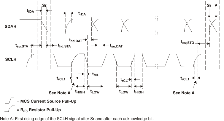 Figure 2. Serial Interface Timing for H/S-Mode
7.7 Typical Characteristics
Table 1. Table of Graphs
| GRAPH NAME | FIGURE NO. | |
|---|---|---|
| LED Power Efficiency | vs Input Voltage | Figure 3, Figure 4 |
| DC Input Current | vs Input Voltage | Figure 5 |
| LED Current | vs LED Pin Headroom Voltage | Figure 6, Figure 7, Figure 8 |
| LED Current | vs LED Current Digital Code | Figure 9, Figure 10, Figure 11, Figure 12 |
| INDLED Current | vs LED Pin Headroom Voltage | Figure 13 |
| Voltage Mode Efficiency | vs Output Current | Figure 14, Figure 15 |
| DC Output Voltage | vs Output Current | Figure 16 |
| vs Input Voltage | Figure 17 | |
| Maximum Output Current | vs Input Voltage | Figure 18 |
| DC Precharge Current | vs Differential Input-Output Voltage | Figure 19, Figure 20 |
| Valley Current Limit | Figure 21, Figure 22 | |
| Balancing Current | vs Balance Pin Voltage | Figure 23 |
| Supply Current | vs Input Voltage | Figure 24 |
| Standby Current | vs Ambient Temperature | Figure 25 |
| Temperature Detection Threshold | Figure 26, Figure 27 | |
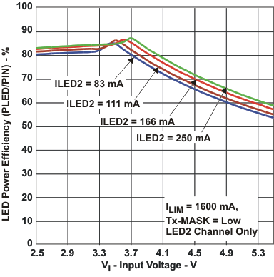 Figure 3. LED Power Efficiency vs Input Voltage
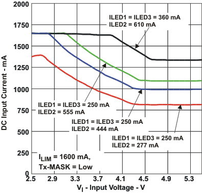 Figure 5. DC Input Current vs Input Voltage
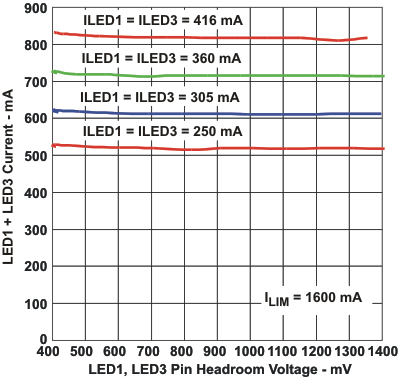 Figure 7. LED1 and LED3 Current vs
LED1 and LED3 Pin Headroom Voltage (HC_SEL = 0)
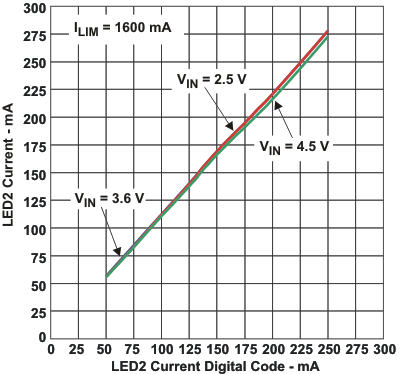 Figure 9. LED2 Current vs
LED2 Current Digital Code (HC_SEL = 0)
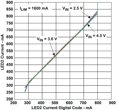 Figure 11. LED2 Current vs
LED2 Current Digital Code (HC_SEL = 0)
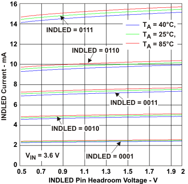 Figure 13. INDLED Current vs
INDLED Pin Headroom Voltage
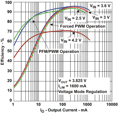 Figure 15. Efficiency vs Output Current
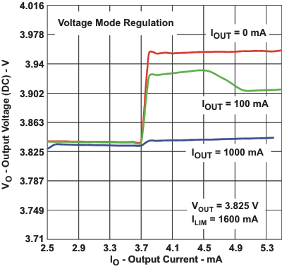 Figure 17. DC Output Voltage vs Input Voltage
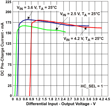 Figure 19. DC Precharge Current vs
Differential Input-Output Voltage (HC_SEL = 1)
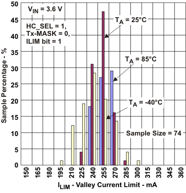 Figure 21. Valley Current Limit (HC_SEL = 1)
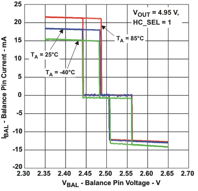 Figure 23. Balancing Current vs Balance Pin Voltage
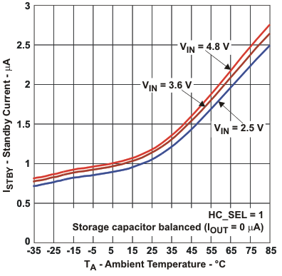 Figure 25. Standby Current vs
Ambient Temperature (HC_SEL = 1)
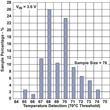 Figure 27. Temperature Detection Threshold
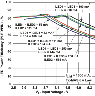 Figure 4. LED Power Efficiency vs Input Voltage
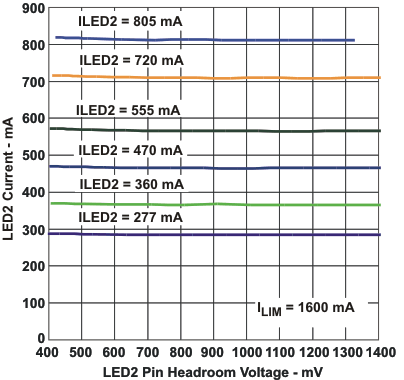 Figure 6. LED2 Current vs
LED2 Pin Headroom Voltage (HC_SEL = 0)
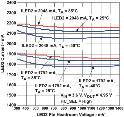 Figure 8. LED2 Current vs
LED2 Pin Headroom Voltage (HC_SEL = 1)
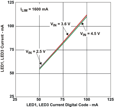 Figure 10. LED1 and LED3 Current vs
LED1 and LED3 Current Digital Code (HC_SEL = 0)
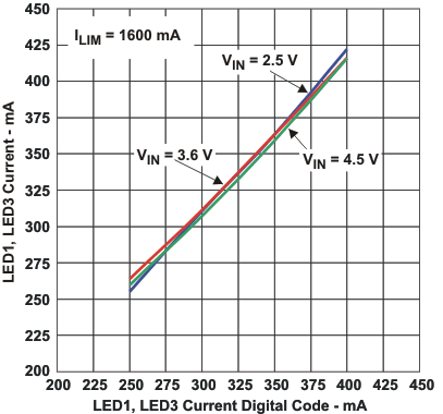 Figure 12. LED1 and LED3 Current vs
LED1 and LED3 Current Digital Code (HC_SEL = 0)
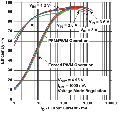 Figure 14. Efficiency vs Output Current
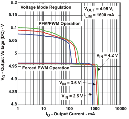 Figure 16. DC Output Voltage vs Load Current
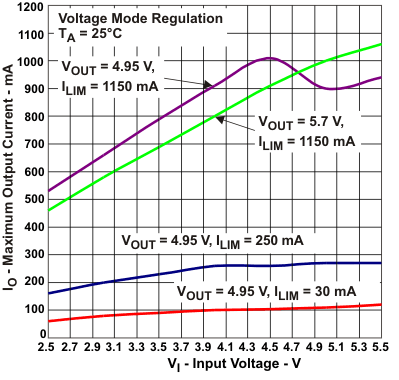 Figure 18. Maximum Output Current vs Input Voltage
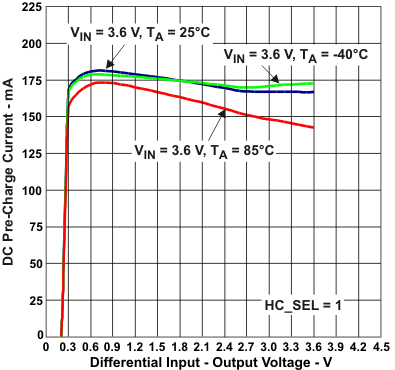 Figure 20. DC Precharge Current vs
Differential Input-Output Voltage (HC_SEL = 1)
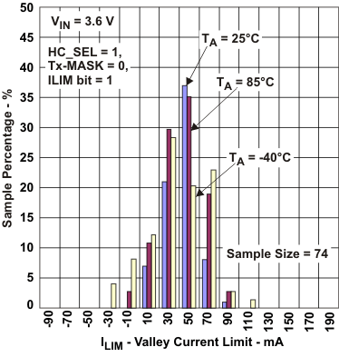 Figure 22. Valley Current Limit (HC_SEL = 1)
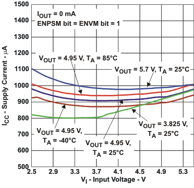 Figure 24. Supply Current vs Input Voltage
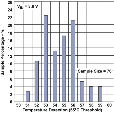 Figure 26. Temperature Detection Threshold