JAJSF66B april   2018  – february 2023 TPS62147 , TPS62148

PRODUCTION DATA  

  1. 特長
  2. アプリケーション
  3. 概要
  4. Revision History
  5. Device Comparison Table
  6. Pin Configuration and Functions
  7. Specifications
    1. 7.1 Absolute Maximum Ratings
    2. 7.2 ESD Ratings
    3. 7.3 Recommended Operating Conditions
    4. 7.4 Thermal Information
    5. 7.5 Electrical Characteristics
    6. 7.6 Typical Characteristics
  8. Parameter Measurement Information
    1. 8.1 Schematic
  9. Detailed Description
    1. 9.1 Overview
    2. 9.2 Functional Block Diagram
    3. 9.3 Feature Description
      1. 9.3.1 Precise Enable
      2. 9.3.2 Power Good (PG)
      3. 9.3.3 MODE
      4. 9.3.4 Undervoltage Lockout (UVLO)
      5. 9.3.5 Thermal Shutdown
    4. 9.4 Device Functional Modes
      1. 9.4.1 Pulse Width Modulation (PWM) Operation
      2. 9.4.2 Power Save Mode Operation (PWM/PFM)
      3. 9.4.3 100% Duty-Cycle Operation
      4. 9.4.4 Current Limit And Short Circuit Protection (for TPS62148)
      5. 9.4.5 HICCUP Current Limit And Short Circuit Protection (for TPS62147)
      6. 9.4.6 Soft Start / Tracking (SS/TR)
      7. 9.4.7 Output Discharge Function (TPS62148 only)
      8. 9.4.8 Starting into a Pre-Biased Load
  10. 10Application and Implementation
    1. 10.1 Application Information
      1. 10.1.1 Programming the Output Voltage
      2. 10.1.2 External Component Selection
      3. 10.1.3 Inductor Selection
      4. 10.1.4 Capacitor Selection
        1. 10.1.4.1 Output Capacitor
        2. 10.1.4.2 Input Capacitor
        3. 10.1.4.3 Soft-Start Capacitor
      5. 10.1.5 Tracking Function
      6. 10.1.6 Output Filter and Loop Stability
    2. 10.2 Typical Applications
      1. 10.2.1 Typical Application with Adjustable Output Voltage
        1. 10.2.1.1 Design Requirements
        2. 10.2.1.2 Detailed Design Procedure
        3. 10.2.1.3 Application Curves
    3. 10.3 System Examples
      1. 10.3.1 LED Power Supply
      2. 10.3.2 Powering Multiple Loads
      3. 10.3.3 Voltage Tracking
      4. 10.3.4 Precise Soft-Start Timing
    4. 10.4 Power Supply Recommendations
    5. 10.5 Layout
      1. 10.5.1 Layout Guidelines
      2. 10.5.2 Layout Example
      3. 10.5.3 Thermal Considerations
  11. 11Device and Documentation Support
    1. 11.1 Device Support
      1. 11.1.1 サード・パーティ製品に関する免責事項
    2. 11.2 ドキュメントの更新通知を受け取る方法
    3. 11.3 サポート・リソース
    4. 11.4 Trademarks
    5. 11.5 静電気放電に関する注意事項
    6. 11.6 用語集
  12. 12Mechanical, Packaging, and Orderable Information

パッケージ・オプション

メカニカル・データ(パッケージ|ピン)
サーマルパッド・メカニカル・データ
発注情報

Pulse Width Modulation (PWM) Operation

TPS62147, TPS62148 have two operating modes: Forced PWM mode discussed in this section and PWM/PFM as discussed in Power Save Mode Operation (PWM/PFM).

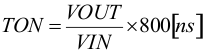
With the MODE pin set to high, the TPS62147, TPS62148 operate with pulse width modulation in continuous conduction mode (CCM) with a nominal switching frequency of 2.5 MHz for FSEL = high and 1.25 MHz for FSEL = low. The frequency variation in PWM is controlled and depends on VIN, VOUT and the inductance. The on-time (TON) in forced PWM mode depends on the setting of FSEL.

For FSEL = high (2.5 MHz):

Equation 1. GUID-3DF26FFC-A0D2-4408-9857-757290881569-low.gif

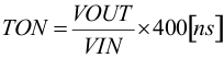
For FSEL = low (1.25 MHz):

Equation 2. GUID-22110EB1-D985-4896-8B0D-398B1740E8E2-low.gif