JAJS355G April 2009 – August 2016 TPS62230
PRODUCTION DATA.
- 1 特長
- 2 アプリケーション
- 3 概要
- 4 改訂履歴
- 5 Device Comparison Table
- 6 Pin Configuration and Functions
- 7 Specifications
- 8 Detailed Description
-
9 Application and Implementation
- 9.1 Application Information
- 9.2
Typical Application
- 9.2.1 Design Requirements
- 9.2.2 Detailed Design Procedure
- 9.2.3
Application Curves
- 9.2.3.1 VOUT = 1.1 V - TPS622311
- 9.2.3.2 VOUT = 1.2 V - TPS62232/TPS62235
- 9.2.3.3 VOUT = 1.8 V - TPS62231
- 9.2.3.4 VOUT = 1.85 V - TPS62236
- 9.2.3.5 VOUT = 2.5 V - TPS62230
- 9.2.3.6 VOUT = 3.0 V - TPS62233
- 9.2.3.7 Start-Up
- 9.2.3.8 PFM / PWM Operation
- 9.2.3.9 Peak-to-Peak Output Ripple Voltage
- 9.2.3.10 Power-Supply Rejection
- 9.2.3.11 Spurious Output Noise
- 9.2.3.12 Line Transient Response
- 9.2.3.13 Mode Transition
- 9.2.3.14 AC-Load Regulation
- 9.2.3.15 Load Transient Response
- 9.3 System Examples
- 10Power Supply Recommendations
- 11Layout
- 12デバイスおよびドキュメントのサポート
- 13メカニカル、パッケージ、および注文情報
パッケージ・オプション
メカニカル・データ(パッケージ|ピン)
- DRY|6
サーマルパッド・メカニカル・データ
- DRY|6
発注情報
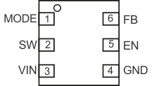
6 Pin Configuration and Functions
DRY Package
6-Pin USON
Top View

Pin Functions
| PIN | TYPE | DESCRIPTION | |
|---|---|---|---|
| NAME | NO | ||
| VIN | 3 | Power | VIN power supply pin |
| GND | 4 | Power | GND supply pin |
| EN | 5 | Input | This is the enable pin of the device. Pulling this pin to low forces the device into shutdown mode. Pulling this pin to high enables the device. This pin must be terminated except for the TPS622319, which has an integrated 1MΩ always active pull-down resistor. |
| SW | 2 | Output | This is the switch pin and is connected to the internal MOSFET switches. Connect the inductor to this terminal |
| FB | 6 | Input | Feedback pin for the internal regulation loop. Connect this pin directly to the output capacitor. |
| MODE | 1 | Input | MODE pin = High forces the device to operate in PWM mode. Mode = Low enables the power save mode with automatic transition from pulse frequency modulation (PFM) to pulse width modulation (PWM) mode. This pin must be terminated except for the TPS622319 , which has an integrated 1MΩ always active pull-down resistor. |