JAJSNC4A november 2021 – may 2023 TPS62441 , TPS62442
PRODUCTION DATA
- 1
- 1 特長
- 2 アプリケーション
- 3 概要
- 4 Revision History
- 5 Device Comparison Table
- 6 Pin Configuration and Functions
- 7 Specifications
- 8 Parameter Measurement Information
- 9 Detailed Description
- 10Application and Implementation
- 11Device and Documentation Support
- 12Mechanical, Packaging, and Orderable Information
パッケージ・オプション
メカニカル・データ(パッケージ|ピン)
- RQR|14
サーマルパッド・メカニカル・データ
- RQR|14
発注情報
6 Pin Configuration and Functions
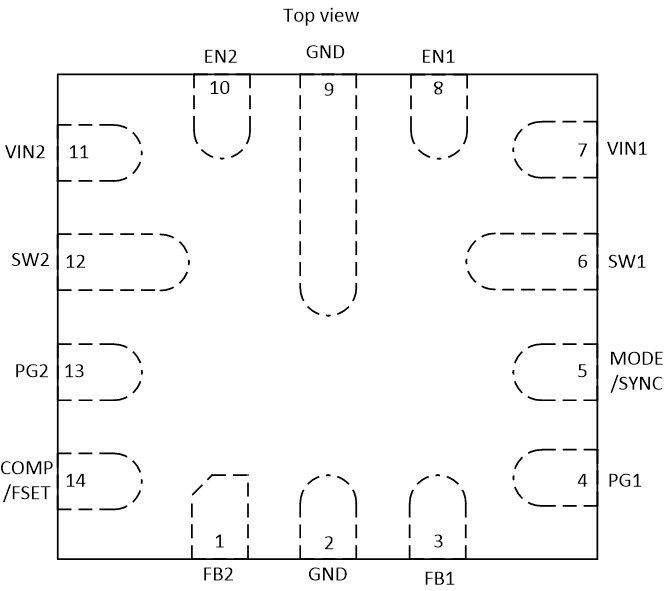
 Figure 6-1 14-Pin QFN RQR Package Top View
Table 6-1 Pin Functions
| PIN | I/O | DESCRIPTION | |
|---|---|---|---|
| NAME | NO. | ||
| EN1 | 8 | I | This pin is the enable pin of converter 1. Connect to logic low to disable the device. Pull high to enable the device. Do not leave this pin unconnected. |
| EN2 | 10 | I | This pin is the enable pin of converter 2. Connect to logic low to disable the device. Pull high to enable the device. Do not leave this pin unconnected. |
| FB1 | 3 | I | Voltage feedback input for converter 1. Connect the resistive output voltage divider to this pin. |
| FB2 | 1 | I | Voltage feedback input for converter 2. Connect the resistive output voltage divider to this pin. |
| PG1 | 4 | O | Open-drain power-good output of converter 1 |
| PG2 | 13 | O | Open-drain power-good output of converter 2 |
| SW1 | 6 | This pin is the switch pin of converter 1 and is connected to the internal power MOSFETs. | |
| SW2 | 12 | This pin is the switch pin of converter 2 and is connected to the internal power MOSFETs. | |
| MODE/SYNC | 5 | I | The device runs in PFM/PWM mode when this pin is pulled low. When the pin is pulled high, the device runs in forced PWM mode. Do not leave this pin unconnected. The mode pin can also be used to synchronize the device to an external frequency. See the electrical characteristics for the detailed specification for the digital signal applied to this pin for external synchronization. |
| COMP/FSET | 14 | I | Device compensation and frequency set input. A resistor from this pin to GND defines the compensation of the control loop as well as the switching frequency if not externally synchronized. Do not leave this pin floating. |
| VIN1 | 7 | — | Power supply input. Make sure the input capacitor is connected as close as possible between pin VIN1 and GND. Connect VIN1 to VIN2. |
| VIN2 | 11 | — | Power supply input. Make sure the input capacitor is connected as close as possible between pin VIN2 and GND. Connect VIN2 to VIN1. |
| GND | 2, 9 | — | Ground pins. The GND pins are internally connected. |