JAJSFX8J August 2018 – March 2023 TPS62810-Q1 , TPS62811-Q1 , TPS62812-Q1 , TPS62813-Q1
PRODUCTION DATA
- 1 特長
- 2 アプリケーション
- 3 概要
- 4 Revision History
- 5 Device Comparison Table
- 6 Pin Configuration and Functions
- 7 Specifications
- 8 Parameter Measurement Information
- 9 Detailed Description
- 10Application and Implementation
- 11Device and Documentation Support
- 12Mechanical, Packaging, and Orderable Information
パッケージ・オプション
メカニカル・データ(パッケージ|ピン)
- RWY|9
サーマルパッド・メカニカル・データ
- RWY|9
発注情報
10.2.2 Detailed Design Procedure
Equation 10. 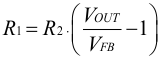
With VFB = 0.6 V:
Table 10-2 Setting the Output Voltage
| NOMINAL OUTPUT VOLTAGE VOUT | R1 | R2 | CFF | EXACT OUTPUT VOLTAGE |
|---|---|---|---|---|
| 0.8 V | 16.9 kΩ | 51 kΩ | 10 pF | 0.7988 V |
| 1.0 V | 20 kΩ | 30 kΩ | 10 pF | 1.0 V |
| 1.1 V | 39.2 kΩ | 47 kΩ | 10 pF | 1.101 V |
| 1.2 V | 68 kΩ | 68 kΩ | 10 pF | 1.2 V |
| 1.5 V | 76.8 kΩ | 51 kΩ | 10 pF | 1.5 V |
| 1.8 V | 80.6 kΩ | 40.2 kΩ | 10 pF | 1.803 V |
| 2.5 V | 47.5 kΩ | 15 kΩ | 10 pF | 2.5 V |
| 3.3 V | 88.7 kΩ | 19.6 kΩ | 10 pF | 3.315 V |