JAJSQ85C november   2011  – september 2020 TPS63060 , TPS63061

PRODUCTION DATA  

  1.   1
  2. 特長
  3. アプリケーション
  4. 概要
  5. Revision History
  6. Device Comparison
  7. Pin Configuration and Functions
    1.     Pin Functions
  8. Specifications
    1. 7.1 Absolute Maximum Ratings
    2. 7.2 ESD Ratings
    3. 7.3 Recommended Operating Conditions
    4. 7.4 Thermal Information
    5. 7.5 Electrical Characteristics
    6. 7.6 Typical Characteristics
  9. Detailed Description
    1. 8.1 Overview
    2. 8.2 Functional Block Diagrams
    3. 8.3 Feature Description
      1. 8.3.1 Power Good
      2. 8.3.2 Soft-Start Function
      3. 8.3.3 Short-Circuit Protection
      4. 8.3.4 Overvoltage Protection
      5. 8.3.5 Undervoltage Lockout
      6. 8.3.6 Overtemperature Protection
    4. 8.4 Device Functional Modes
      1. 8.4.1 Buck-Boost Operation
      2. 8.4.2 Control Loop
      3. 8.4.3 Power-Save Mode
      4. 8.4.4 Synchronization
      5. 8.4.5 Dynamic Voltage Positioning
      6. 8.4.6 Dynamic Current Limit
      7. 8.4.7 Device Enable
  10. Application and Implementation
    1. 9.1 Application Information
    2. 9.2 Typical Application
      1. 9.2.1 Design Requirements
      2. 9.2.2 Detailed Design Procedure
        1. 9.2.2.1 Step One: Output Filter Design
        2. 9.2.2.2 Step Two: Inductor Selection
        3. 9.2.2.3 Step Three: Capacitor Selection
          1. 9.2.2.3.1 Input Capacitors
          2. 9.2.2.3.2 Output Capacitor
          3. 9.2.2.3.3 Bypass Capacitor
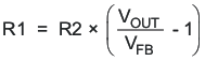
        4. 9.2.2.4 Step Four: Setting the Output Voltage
      3. 9.2.3 Application Curves
  11. 10Power Supply Recommendations
  12. 11Layout
    1. 11.1 Layout Guidelines
    2. 11.2 Layout Example
  13. 12Device and Documentation Support
    1. 12.1 Device Support
      1. 12.1.1 Development Support
    2. 12.2 Documentation Support
      1. 12.2.1 Related Documentation
    3. 12.3 Receiving Notification of Documentation Updates
    4. 12.4 Community Resources
    5. 12.5 Trademarks
  14. 13Mechanical, Packaging, and Orderable Information

パッケージ・オプション

メカニカル・データ(パッケージ|ピン)
サーマルパッド・メカニカル・データ
発注情報

Step Four: Setting the Output Voltage

When the adjustable output voltage version TPS63060 is used, the output voltage is set by the external resistor divider. The resistor divider must be connected between VOUT, FB and GND. When the output voltage is regulated properly, the typical value of the voltage at the FB pin is 500mV. The maximum recommended value for the output voltage is 8V. The current through the resistive divider should be about 100 times greater than the current into the FB pin. The typical current into the FB pin is 0.01 μA, and the voltage across the resistor between FB and GND, R2, is typically 500 mV. Based on these two values, the recommended value for R2 should be lower than 500 kΩ, in order to set the divider current at 3 μA or higher. It is recommended to keep the value for this resistor in the range of 200 kΩ. From that, the value of the resistor connected between the VOUT pin and the FB pin, (R1) depending on the needed output voltage can be calculated using Equation 6.

Equation 6. GUID-21E6AFD1-828E-4B58-BAA8-F67C0476108F-low.gif

Place a small capacitor (C4, 10 pF) in parallel with R2 when using the power save mode and the adjustable version, to provide filtering and improve the efficiency at light load.