JAJSNI5A december 2022 – august 2023 TPS631010 , TPS631011
PRODUCTION DATA
- 1
- 1 特長
- 2 アプリケーション
- 3 概要
- 4 Revision History
- 5 Device Comparison Table
- 6 Pin Configuration and Functions
- 7 Specifications
-
8 Detailed Description
- 8.1 Overview
- 8.2 Functional Block Diagram
- 8.3 Feature Description
- 8.4 Device Functional Modes
- 9 Application and Implementation
- 10Device and Documentation Support
- 11Mechanical, Packaging, and Orderable Information
9.2.2.4 Setting the Output Voltage
The output voltage is set by an external resistor divider. The resistor divider must be connected between VOUT, FB, and GND. The feedback voltage is 500 mV nominal.
Keep the low-side resistor R2 (between FB and GND) below 100 kΩ. The high-side resistor (between FB and VOUT) R1 is calculated with Equation 4.
Equation 4. 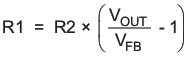
where
- VFB = 500 mV
Table 9-5 Resistor Selection For Typical Output Voltages
| VOUT | R1 | R2 |
|---|---|---|
| 2.5 V | 365K | 91K |
| 3.3 V | 511K | 91K |
| 3.6 V | 562K | 91K |
| 5 V | 806K | 91K |